Understanding PCB Ink Types and Properties: Eco-Friendly Production

directory

What is PCB ink?

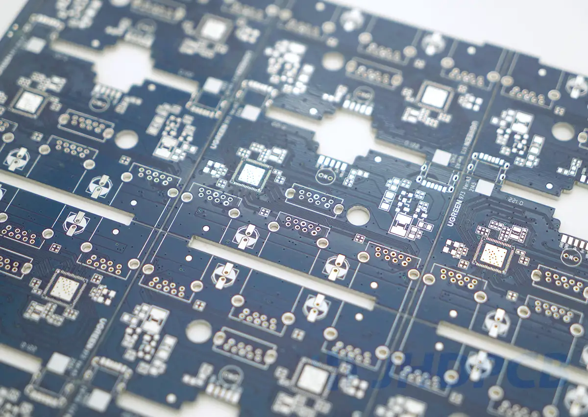
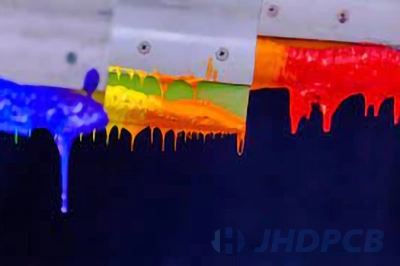
PCB inks are inks that are used on printed circuit boards (also known as PCBs), and they have essential physical features like viscosity, thixotropy, and finesse. Frequently widely utilized for printing, marking, and other uses.
There are three main categories of PCB ink,which are:PCB etching ink, Solder mask Ink and PCB silkscreen ink.These are all very common in PCB production.There are also inks like conductive carbon oil and conductive silver oil (they are also known as conductive carbon ink and conductive silver paste). In general, conductive ink for PCB are not as common as other PCB inks.And there’s things like PCB marking ink which we’re not gonna going deep into today.

PCB ink

What are the common types of PCB inks?

Today, we will be talk about three kinds of PCB inks,and they are all pretty common in our daily life,which are:

  • Etching Ink;
  • Solder mask Ink;
  • PCB silkscreen ink;

Etching Ink:

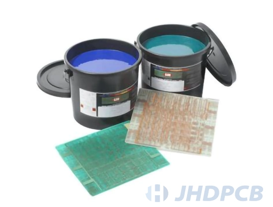
Let’s take a look at the first one: PCB circuit etching ink. There is a layer of copper foil on top of the substrate of the PCB, which is a copper clad laminate. It must be screen-printed, and photosensitive etching ink is required during the process. And then is the exposure and development, so that we can let the unexposed spots etch away. Then the final step is fade. This line etching ink is mostly used for protection. The sodium hydroxide aqueous solution will be used to remove the ink after the line has been etched. Due to the fact that most circuit board etching inks are blue, they are also known as photosensitive blue oil or circuit blue oil. This type of ink is also used in some hardware stainless steel etching. And it is referred to as photosensitive glue by some people. As for the photosensitive glue which used for the plate, there appears to be a significant difference. View more detailed PCB etching information.

Etching Ink

Solder mask Ink:

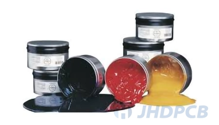
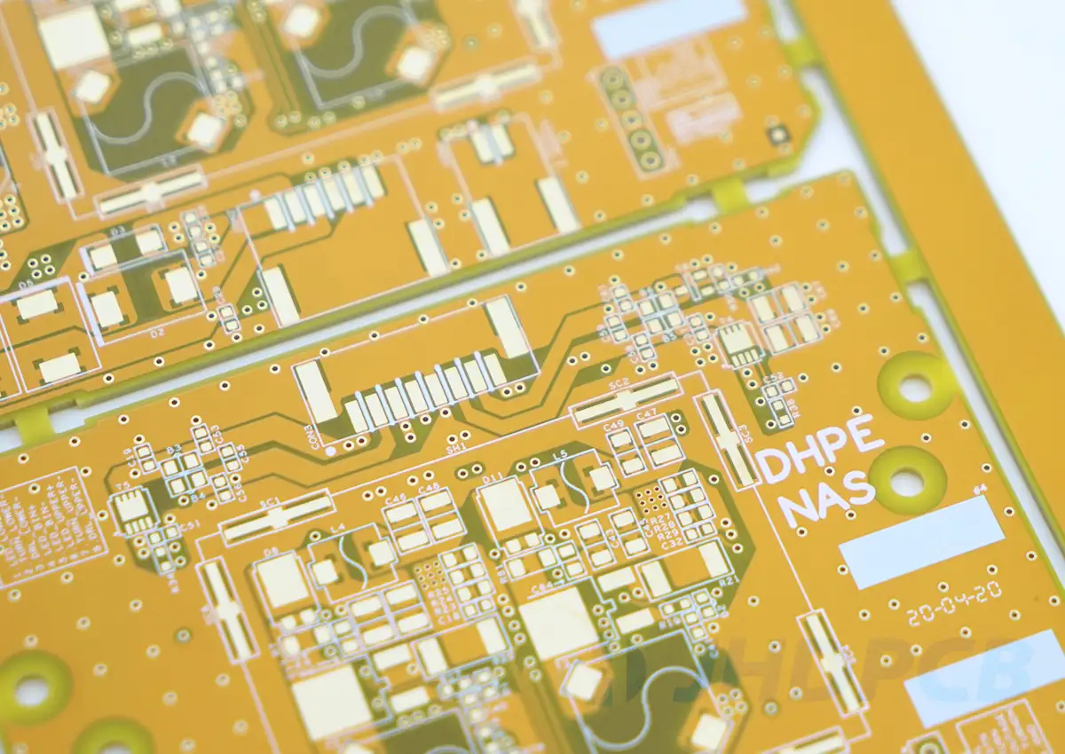
Now, moving on to the second one, which is PCB circuit board solder mask, also known as solder mask ink or PCB masking ink. Solder mask ink is something that people often see or use on the PCB circuit board. When you see the circuit board is covered in a layer of green paint, you’ll know is solder mask ink.
With different curing methods, PCB masking ink can be different too. If it’s thermally cured, it will be thermosetting inks, and if it’s cured by UV light, then it will be UV curable inks. Also, there are photosensitive developing inks.
And with different boards, there are different categories. Which are aluminum substrate solder mask ink, PCB hard board solder mask ink, and FPC soft board solder mask ink. Ceramic boards can also use aluminum substrate solder mask ink on them.
Ultraviolet light cures the photosensitive solder resist ink. First step, pre-baked the thing. And then, it needs to be exposed. Finally, it can be developed. It is typically used to create different PCB hard boards. For circuit boards with precise pads on soft boards, photosensitive solder resist inks is one of the option, you can also use dry film. After printing, the thermosetting ink should be baked directly. The two most popular ones are white solder mask ink for light bar boards and mobile phone antenna board ink.UV green oil is more popular among the other UV curable inks, and it’s typically used in circuit boards that don’t require much, or in circuit boards that are produced in automated manufacturing lines. The requirements for photosensitive ink are relatively high in comparison to UV curable inks, photosensitive ink, and thermosetting ink, with UV curable inks coming in last. In general, There are higher precision with the photosensitive ink while poor adhesion that is with UV curable inks.

Solder mask Ink

PCB silkscreen Ink:

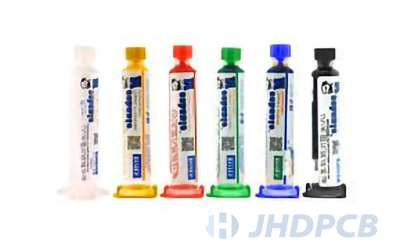
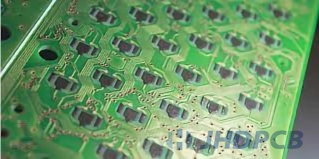
PCB silkscreen ink or Silk Screen Printing Ink is basically a layer of ink traces that is used to identify things like parts of the PCB, warning symbols, logos and marks, test points, components and so on. The silkscreen is single-sided, it is usually placed to the component side, nevertheless, you can see it on the solder side quite often too. However, this might makes it cost more than others. In general, a thorough and complete PCB silkscreen can assist the engineer and the PCB manufacturers in finding and recognizing all the components. Standard fonts are also used by PCB software in multi layers of silkscreen, however you have the option to select another font from the system. A polyester screen stretched over aluminum frames, a laser photo plotter, spray developer, and curing ovens are needed for standard silk screening. This peculiar epoxy-based ink is non-conductive and quite distinct from traditional printing ink. Up to now, The most preferred ink color for screen printing process is white. Other common options for ink are yellow and black. View more detailed PCB silkscreen information.

PCB silkscreen Ink

How to judge the performance of PCB ink?

Viscosity and thixotropy:
Screen printing is one of the vital procedures required for the production of printed circuit boards. Ink needs to have high adherence and the right thixotropy in order to replicate an image with accuracy.
As you might wonder, what is this thing called ‘viscosity’?To break it down, when a liquid layer slides over another layer under the influence of an external force, the inner layer of the liquid generates friction force, which we call that internal friction, and this multi layer process also called ‘viscosity’.
The inner layer of thick liquid receives more mechanical resistance while sliding while the resistance of the thinner liquid is less. Poise is the unit when you measure the viscosity. It is important to recognize that viscosity is significantly influenced by temperature.
Thixotropy is actually one of the physical appearances of liquid, it refers to the fact that the liquid loses viscosity when stirred and soon recovers it when left still. Thixotropy’s long-lasting effects during stirring are adequate to remodel the inner structure. The thixotropy of the ink is crucial for producing high-quality screen printing effects. The ink is stirred up to make it liquefy, especially during squeegee, which is one of the processes. This effect helps speed up the ink’s flow through the mesh, and the ink that is separated by the mesh will be connected more quicker because of it. The ink returns to a static condition when the squeegee stops moving, and its viscosity quickly reaches the original needed data.

Finesse:
Mineral fillers and pigments are usually solid substances. Their particle size is less than 4/5 microns after fine grinding, and they create a homogenous fluid condition in solid form. Hence, it is essential to ensure that ink is fine.

Plasticity:
It indicates that even after being bent by an outside force, the ink has its original form. The ink’s flexibility aids in enhancing printing accuracy.

Fluidity:
It basically means how much the ink spreads when exposed to outside stress. The opposite of viscosity is fluidity, which is related to the ink’s plasticity and thixotropy. When the plasticity, thixotropy and fluidity are large, then the imprint is easy to spread. When the fluidity is poor, it’ll make the netting likely to appear and cause the ‘netting’, or as known as the ‘ink knotting phenomenon’.

Viscoelastic:
It means the ink on the squeegee blade, the shear fracture of the ink led to an immediate rebound performance. Ink must have a high rate of deformation, rebound speedily, and be suitable for printing.

Dry:
It required the needed ink slowly dried on the screen, but when the ink is moved to the substrate, it need to be ASAP.

Fineness:
PCB ink’s dyes and solid substance’s particle size is typically less than 10 m; its diameter should be smaller than the third-finest mesh opening.

Transparency and Opacity:
For PCB ink, different demands were made depending on the application and needs for transparency and opacity inks.
Line ink, PCB conductive ink, and ink characters should have a high level of hiding power. A more flexible solder resist is available.

Inks chemical resistance:
With various purposes, PCB has various needs and strict standards for the related acids, bases, salts, solvents and so on.

Resistance to the ink’s physical features:
PCB ink must meet a number of demanding electrical performance standards, as well as requirements for exterior scratch resistance, thermal stress, and mechanical stripping.

Use of safe and environmentally friendly inks:
PCB needs to be hypotoxicity, unscented, secure and environmental friendly.

The latest eco-friendly ink PCB: carbon ink PCB.

What is Carbon Ink PCB?

Carbon ink PCBs, also known as carbon conductive ink for PCB. A circuit board in which carbon ink is applied to copper pads, replacing some of the more typical solder plating techniques such as electroless nickel immersion gold (ENIG) or hot air solder levelling.
With the market’s needs for PCB board production costs having decreased frequently, carbon oil keys are starting to replace the pricey gold keys. As for the single and double PCBs, carbon oil board became a pretty popular surface finishing technique because of its environmentally friendly features. After a number of examinations such as aging tests, and other technical operations.It is proved that the PCB can function stably for a very long period.

Carbon Ink PCB

Carbon Ink PCB features and applications.

Carbon Ink PCBs excel in the use of rubber keypads, which are often seen in television remote controllers, garage door controllers, and other electronic devices that involves rubber keypads. In a standard conductive rubber keypad, the switch center is encircled by angled webbing. The webbing deforms and generates a tactile feedback when the switch is pressed. The webbing returns to its neutral state when the switch is no longer under pressure.
When manufacturing electrical switches, the carbon tactile key is used because a carbon pill is positioned at the base of the switch center. If you’ve ever disassembled (or damaged) a Television remote control, you might just have noticed that on the printed circuit boards, underneath each rubber button you pressed, there was a tiny round dot that could be easily pushed down. When the web is pushed, this carbon tactile key makes contact with the PCB; it’s an easy but relatively straightforward solution that is also long-lasting and economical.

Suggested storage method for PCB ink.

The majority of PCB manufacturers have found that when using ink, the following guidelines must be followed:

  • To retain the ink’s quality, it is best for you to keep or store it at ambient temperature in the process settings. In order for the ink tank to reach the ideal operating temperature when ink is stored outside or at different temperatures, it needs to be exposed to the air temperature for a couple of days before using. This is because cold ink will cause screen printing malfunction and require extra labor.
  • If the temperature is higher than 20-25°C, the viscosity of the ink and thus the quality of the screen printing will be affected, so remember to always keep the temperature below this range.
  • The ink must be properly mixed either manually or mechanically before use.
  • Leave the ink to sit for a bit before using it if air has gotten into it.
  • If it needs to be diluted, thoroughly mix it before evaluating its viscosity.
  • The ink tank must be immediately closed after each use. Also, if there’s unused ink in the ink tank, keep in mind that never ever blend it with the ink on the screen.
  • Cleaning the net should be done properly and neatly with mutually compatible cleaning solutions. When cleaning it once again, it is best to use a clean solvent.

There are still a couple of things that you should remember, The ink must be dried in a piece of equipment with a reliable exhaust system. And also, screen printing needs to be done in an environment that exceeds the technical requirements of the process in order to maintain operational conditions.

Common problems and countermeasures in the use of PCB ink.

Problems Countermeasures

Not enough time for ink mixing

Ink mixing mishap

Board water or oil stains (pre-treatment unclean)

Impurities in ink (oil mixed tape and damage the surface tension)

Negative scraping film component

Unhygienic screen cleaning

Expired ink mixed after usage

To ensure the drying operation’s drying section is of high quality, check the pre-treatment line.

Verify that the pre-treatment procedure adheres to the requirements of the paragraphs (water breaking , grinding marks)

Examine the ink-mixing conditions.

Cleaning screens instead of using implements like scrapers.

make sure the screen is clean,and replace the use of tools such as scrapers.

Inadequate pre-treatment

Impurities on the plate’s surface

Surface downturns in copper

Can’t mix the ink

Copper surface ink has an unequal thickness

The ink surface has been impacted

Oven temperature and baking time insufficient or uneven overbake

Examine the pre-treatment line to ensure that the working section can meet the quality standards.

Check the baking temperature and temperature distribution curve in the oven.

Examine mixing parameters of the ink.

Examine the manufacturing process to minimise the external effect.

Ensure that the HAL job parameters and settings are correct.

The ink is way too weak

Insufficient baking

The soaking time of flux is too long

The flux is too intense

The temperature of the spray tin is way too high

Change the solder printing thickness.

Decrease the thickness of the line plating.

Check conditions  of the oven baking.

Verify the HAL job parameters and settings.

Examine the manufacturing process to minimise the external effect.

Check the pre-treatment line drying quality requirements.

Poor vacuum pump exposure

The positioning piece has not been placed into the hole

Instability of vacuum suction pressure

Debris caught to the film

Use job boards that are thinner than the air guide bar.

Securely inserted into the positioning hole.

Examine the negatives and conduct an independent inspection.

There is no section for heating

The temperature of the low-temperature heating section is too high.

Insufficient time to warm up the cold section.

The baking temperature is not stable in one section.

The oven temperature is uneven.

The heating needs for continuous baking.

The oven needs to heat up the curve areas.

The heated air must be directed in the same direction.

Verify job parameters.

The temperature of the heating section is too low.

Insufficient time for the heating section.

The temperature in the oven is unequal.

No pre- heated baking.

Check the oven temperature for each section.

Check the baking operation parameters after that.

Confirm the HAL operational parameters and conditions.

If you don’t know which ink is needed for your current PCB application. You can send your Gerber files through our quotation page, we will provide the best suggestion according to your application conditions and PCB design. You will get high-quality PCB manufacturing services from JHDPCB, whether it is ink or other production links. JHD always strictly controls every production step. If you want to learn more about printed circuit boards, don’t forget to visit our other blogs for more interesting content about the PCB industry.

Get a PCB Quote Now

Open high-quality PCB manufacturing services in JHDPCB

Leave a Comment