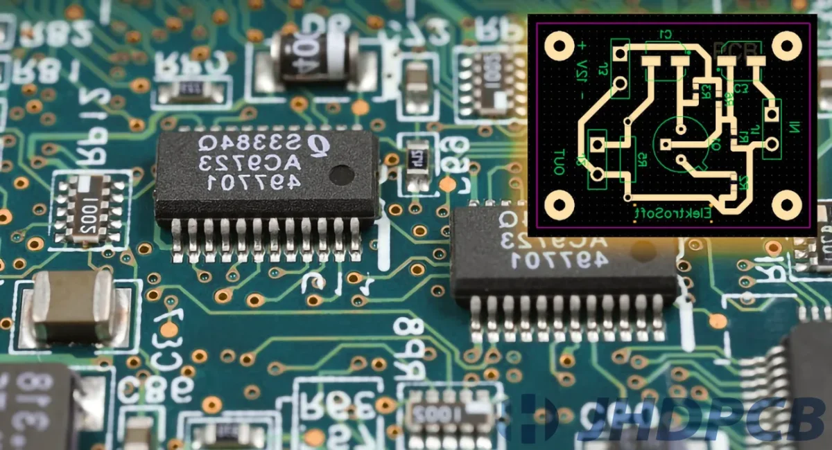
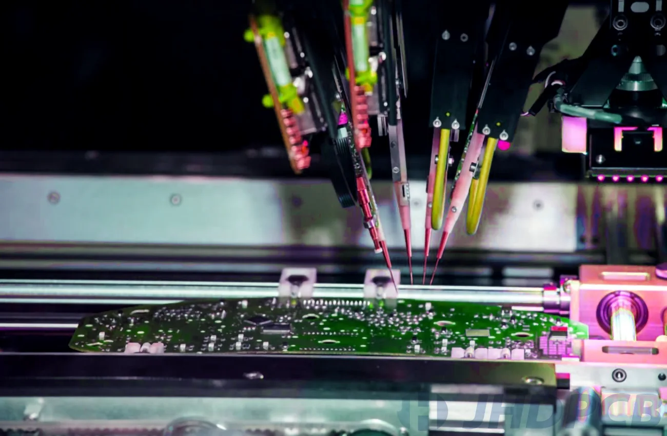
PCB Gerber Files: Ultimate Guide for Beginners.
jhdpcb@gmail.com
What is a Gerber file?
A Gerber file is a file format that includes information used to guide the manufacturing process of a PCB. Gerber files have been in use since the 1960s and were named after their inventor, H. Joseph Gerber. They are now a widely accepted standard in the industry, and virtually all PCB design software packages can generate Gerber files.
The Gerber format is a type of file format utilized to depict the picture of a PCB. It is essentially a 2D coordinate file that characterizes each layer of the board. In addition to copper traces, drill holes, and silkscreen layers, Gerber files also cover knowledge about solder mask layers, paste layers, and surface mount pads. The compilation of layers contained in a Gerber file can fluctuate relying on the specific requirements of a given PCB design.
The accuracy and precision of a Gerber file are vital for PCB production. PCB manufacturers rely on this file to guide the manufacturing equipment, with even slight errors or inconsistencies leading to critical defects in the final product. As such, designers must ensure that the Gerber file they produce precisely reflects the intended design and follows the manufacturer’s specifications.
Despite its importance, a Gerber file is just one part of the PCB fabrication process. Additional essential stages include design validation, manufacturing preparation, assembly, and testing. PCB designers must maintain close communication with manufacturers throughout each stage to ensure that the final product satisfies their expectations. Overall, the Gerber file is an essential element in PCB design, reflecting the significance of meticulous planning and attention to detail in producing high-quality electronic components.
How Gerber Files Are Used In PCB Manufacturing?
Gerber files are utilized in the PCB fabrication process, being read by manufacturing equipment to produce each layer of the PCB. PCB Gerber provides exact and precise details of the PCB design, guaranteeing that the final product fulfills all design requirements. The following are the main uses of Gerber files in the production of printed circuit boards (PCBs):
- Design validation: Gerber files facilitate a pre-production DFM review of the design layout of the board before manufacturing to identify and correct any errors or issues that could result in costly mistakes during production.
- Photolithography: Gerber files are utilized to generate photolithographic image films that are used to produce physical PCBs. The Gerber files direct the UV-sensitive material’s precise exposure on the film, which is developed to etch the copper traces and other features onto the board. View more detailed PCB etching process.
- Drilling: Gerber files are also used to guide the drilling of the holes on the PCB, ensuring that the drill head is accurately positioned to create precise drill holes according to the design specifications.
- Solder mask application: Gerber files contain information about the solder mask layer that protects the board from unwanted solder bridges forming between adjacent leads and prevents damage to the copper traces during the soldering process.
- Silk screen printing: Gerber files include data regarding the silk screen layer, which enables the printing of additional information, such as component reference designators and logos, on the top and bottom of the board.
Gerber files are an indispensable element in PCB manufacturing, with their precision and comprehensiveness being key to the successful production of top-quality PCBs. JHDPCB boasts significant expertise in creating Gerber files that align with stringent quality standards, providing our clientele with dependable and economical PCB solutions.
What should the Gerber file contain?
The Gerber file should contain all the necessary information to manufacture a printed circuit board (PCB) accurately. This includes:
- Copper Traces and Pads on Top and Bottom Layers: The upper layer houses most components and copper traces, while the bottom layer holds ground planes and other traces that can’t fit on the top one. The Gerber file should provide elaborate information on both layers to ensure successful manufacturing.
- Top and Bottom Solder Mask Layers: Solder mask layers are essential in preventing shorts between copper traces, pads, and components. Gerber files should contain specific data on the coverage of solder masks on the top and bottom layers.
- Silkscreen Layers on Both Top and Bottom: Silkscreen layers offer visual cues for precise component placement during PCB assembly. Gerber files should specify the size and location of labels, symbols, and other silkscreen markings on both top and bottom layers.
- Drill Hole Patterns and Locations: Drill hole patterns and locations are crucial in PCB design and must be included in the Gerber file. Drill files provide manufacturers with patterns, hole sizes, and other details necessary for drilling holes in the PCB.
- Continuous Copper Connections: Copper pours are large areas of continuous copper connections designed to enhance the electrical performance of the PCB. The Gerber file should indicate the copper pour size and placement on both top and bottom layers.
- Board Dimensions and Outline: The Gerber file must detail the board’s outline, including dimensions, shape, and cutouts for connectors, displays, or other components.
- Drill Hit Markings: Gerber files may include drill hit markings, which indicate where the drill bit should hit during drilling to ensure precise hole placement, in addition to information about holes and their locations.
- Hidden and Buried Vias: These types of vias are utilized to connect different layers of the PCB without passing through all layers and require special manufacturing techniques. Gerber files should provide information on the placement and size of hidden and buried vias on the PCB.
- PCB Panelization: If the PCB design includes multiple copies of the same circuit, Gerber files may be combined into a panel for mass production. The Gerber file should detail the panel layout and the number of circuit copies included in each panel.
- PCB Surface Treatment: The Gerber file may contain information about the PCB’s surface finish or specific areas of the board. Surface treatment can impact the PCB’s performance and the solderability of components.
In conclusion, the Gerber file is a crucial component in creating a PCB that meets the designer’s specifications, containing all essential information required by manufacturers to produce high-quality PCBs. It’s noteworthy that an organized and properly formatted Gerber file can significantly enhance the manufacturer’s ability to achieve this.
What are the different extensions for Gerber files?
- .gbr or .ger: These are the most common extensions used for Gerber files. They contain information about the different layers of a PCB design, including copper traces, drill holes, and silkscreen layers.
- .pho:This extension is sometimes used for photoplotter output files, which are similar to Gerber files and contain the same type of information.
- .topand .bot: These extensions are often used to differentiate between the top and bottom layers of a PCB design.
- .smtand .smb: These extensions indicate the solder mask top and solder mask bottom layers of a PCB design, respectively.
- .cmp: This extension is sometimes used for the top layer of a PCB design that shows the components.
- .plc: This extension is sometimes used for the top layer of a PCB design that shows the placement of components.
- .sol: This extension is sometimes used for the bottom layer of a PCB design that shows the copper traces.
- .stc: This extension is sometimes used for the top layer of a PCB design that shows the solder stencil information for stencil printing.
- .sts: This extension is sometimes used for the bottom layer of a PCB design that shows the solder stencil information for stencil printing.
- .drd: This extension is used to indicate drill data for a PCB design that shows where the holes should be drilled into the board.
| Gerber File | Description | Contents |
|---|---|---|
| .GTL | Top layer copper | Copper traces and pads on the top layer |
| .GTS | Top layer solder mask | Shape of the solder mask on the top layer |
| .GTO | Top Overlay | Top layer silkscreen information such as component identification |
| .GBL | Bottom layer copper | Copper traces and pads on the bottom layer |
| .GBS | Bottom solder mask | Shape of the solder mask on the bottom layer |
| .GBO | Bottom layer Overlay | Bottom layer silkscreen information |
| .GTP | Top layer paste | Location of solder paste on the top layer |
| .GBP | Bottom layer paste | Location of solder paste on the bottom layer |
| .GML | Mechanical layer | Board cutouts, drill holes, and non-copper features |
| .GKO | Keep-out layer | Areas where components or copper traces cannot be placed |
| .G1 to .Gx | Additional copper layers | Additional copper layers for multilayer designs |
| .GP1 to .GPx | Additional Internal Plane Layer | Additional Internal Plane Layer for multilayer designs |
| Other pcb Gerber file extension tables | |
|---|---|
| File Extension | Description |
| .P01 to .P0x | Gerber Panels |
| .GM1 to .GMx | Mechanical Layer |
| .GD1 to .GDx | Drill Drawing |
| .GG1 to .GGx | Drill Guide |
| .GPT | Pad Master Top |
| .GPB | Pad Master Bottom |
| .APR/.APT | Aperture File |
| .EXTREP | Extension Report of Gerber Files |
| .REP | Report of Individual Layer Used Aperture List |
| .RUL | DRC Rules |
The type of gerber file extensions used for PCB design may differ based on the specific software employed, but they tend to adhere to a common naming convention that indicates the data embodied in each file. Gerber files are crucial to the PCB manufacturing process, guaranteeing the accurate production of boards that conform to design requirements.
JHDPCB is a trustworthy and efficient provider of PCB fabrication and assembly services, recognizing that accurate and comprehensive data is vital to producing top-notch PCBs. Our modern PCB production facility is equipped with cutting-edge software and equipment to guarantee that every PCB we manufacture adheres to stringent requirements.
Gerber file formats from ancient times to the present.
Over the years, Gerber file formats have progressed from the original RS-274-D format to the current Gerber-X2 format. Here’s a concise summary of each Gerber file format:
RS-274-D:
RS-274-D is the first Gerber file format developed by Gerber Scientific Products in the 1960s. It is a binary file format that represents PCB design information as a set of commands, each command comprising a specific instruction and data for that instruction. RS-274-D is still in use today, though with the introduction of more advanced Gerber formats like Gerber-X2, it is less common.
The format is based on a matrix of “dots” or “pels” (picture elements), which describes the geometries of the PCB. Each pel is defined by a location within the matrix, and a “state” — either “on” or “off”. The pels are arranged in a rectangular grid, with the first pel located at the origin (0, 0). The X and Y coordinates of each pel are encoded in ASCII, in thousandths of an inch or millimeter.
RS-274-D is divided into two main sections: the aperture list and the drawing list. The aperture list contains definitions of the “tools” used to create the circuits, while the drawing list specifies the actual data to be drawn using those tools.
The aperture list contains the definitions of the aperture shapes, sizes, and features used to draw the PCB. The aperture list uses a series of commands to define the size and shape of each aperture, followed by a description of the actual data that will be drawn using that aperture. The aperture list also includes commands to define the units of measurement used for the data.
The drawing list specifies the actual data to be drawn using the tools defined in the aperture list. The data is represented as a series of commands, each starting with an X and Y coordinate and followed by a command code. The command code determines what type of object is being drawn, with codes for lines, arcs, circles, and other shapes.
Despite its limitations, RS-274-D is still used in some cases, particularly for simple PCB designs. However, more advanced Gerber formats like Gerber-X2 have largely replaced it due to their improved functionality and ease of use.
RS-274-X:
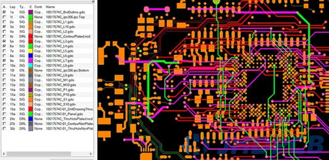
RS-274-X is an improved version of the RS-274-D Gerber file format. It was introduced in the 1980s as a replacement for RS-274-D, and added support for aperture definitions, allowing for more complex geometries. The format was developed to provide a standardized way to communicate PCB designs to manufacturing facilities.
The RS-274-X format’s crucial aspect is its capability to specify apertures.An aperture is a tool used to create shapes on a PCB, such as a circle or a rectangle. In RS-274-X, aperture definitions are included within the data file and use a syntax similar to the drawing commands. An aperture consists of either a simple shape defined by its size or a more complex shape defined by a custom “macro”.
Another improvement in RS-274-X is the use of ASCII characters in place of the binary data used in RS-274-D. This made it easier for PCB designers to view and edit files using common text editors. The new format also allowed designers to include comments in the data file, making it easier to understand the intention behind their designs.
RS-274-X has several commands that help to describe the PCB layout in more detail. For example, G01 is a command used to draw a line, while G02 and G03 are used to draw arcs. D codes specify the aperture to be used for each segment. A D code is a two-digit number that corresponds to an aperture definition in the aperture list.
Overall, RS-274-X improved upon the limitations of the previous RS-274-D format and became the industry standard for Gerber file formats for many years. However, as PCB design software has continued to evolve, newer file formats like Extended Gerber (XGerber) and Gerber-X2 have been developed to meet the needs of more complex PCBs.
Extended Gerber (XGerber):
Extended Gerber (XGerber) is a Gerber file format that was developed to extend the capability of the original Gerber format (RS-274-D). It was created to address some of the limitations of the RS-274-D format and provide additional features and functionality for PCB designers.
The XGerber format introduces several enhancements over the RS-274-D format, such as support for aperture macros, which allow users to define complex apertures and reuse them throughout the design. The format also includes support for different fill types, allowing designers to control the fill area of polygons or planes in their designs.
Another important feature of the XGerber format is its support for embedded data, which enables designers to include additional information such as drill and rout data directly in the Gerber files. This eliminates the need for separate files and simplifies the fabrication process.
Like the RS-274-D format, the XGerber format consists of a series of commands that describe the geometries of the circuits, with each command containing specific instructions and data for that instruction. The commands are based on a set of Gerber codes, which are standardized by the IPC (Association Connecting Electronics Industries).
Overall, the Extended Gerber (XGerber) format has become widely used in the PCB industry due to its enhanced functionality and compatibility with modern PCB design tools.
Gerber-X2:
Gerber X2 is a newer Gerber file format that was developed to provide an even greater level of functionality and compatibility with modern PCB design tools than the previous Gerber formats. It was introduced to address some of the limitations of the older Gerber formats and provide additional features and capabilities that were not present in those formats.
The Gerber X2 format includes support for multiple layers, embedded aperture information, and various fill types. It also provides the ability to include meta-information, such as PCB layer structure, trace width, and drill sizes, directly in the Gerber files. This eliminates the need for separate documentation and simplifies the manufacturing process.
One of the key features of the Gerber X2 format is its support for metadata tags, which enable designers to include additional information related to the PCB design, such as supplier information, material specifications, and assembly instructions. The format also includes support for the use of XML-based data structures, which allows the information in the Gerber files to be more easily managed and exchanged between different software applications.
Like the previous Gerber formats, the Gerber X2 format consists of a series of commands that describe the geometries of the circuits, with each command containing specific instructions and data for that instruction. The commands are based on a set of standardized codes developed by the IPC (Association Connecting Electronics Industries).
Overall, the Gerber X2 format has gained widespread adoption in the PCB industry due to its enhanced functionality and compatibility with modern PCB design tools. It has become the preferred format for many designers and manufacturers who require accurate and reliable data exchange between different stages of the PCB design and manufacturing process.
In addition to these formats, there are also several vendor-specific Gerber formats that have been developed over the years. However, the industry has largely standardized on the Gerber-X2 format as the preferred format for exchanging PCB design data.
Essential features of a Gerber file viewer.
A software application that enables users to examine and view Gerber files, utilized in PCB fabrication, is known as a Gerber file viewer. An excellent Gerber file viewer should comprise the following key attributes:
- Accurate Display: The Gerber file viewer should accurately and correctly display the Gerber files. It should allow users to zoom, rotate and pan the view to inspect the design in detail.
- Layer Control: The viewer should be capable of managing different layers of the Gerber files, such as copper layers, solder mask layers, legend layers, and drill files. It should allow users to adjust transparency levels and toggle layers on and off.
- Precision Tools: The viewer should include different precision tools that enable users to take accurate measurements of distances, angles, and other attributes of the design.
- Annotation Features: The viewer should provide the ability to add notes, labels, and other annotations to the design. It should have easy-to-use markup features that enable users to highlight specific areas of interest.
- File Compatibility: The viewer should support a wide range of Gerber file formats, including newer ones like Gerber X2, as well as other formats such as DXF, DWG, and PDF.
- User-Friendly Interface: The viewer should have a user-friendly interface that is easy to use and allows users to navigate through the design quickly and efficiently.
- Export Options: The viewer should have the functionality to export the design in various file formats, such as PDF or PNG, making it simple for users to share with others.
- Latest File Format Support: The viewer should support the latest Gerber file formats, like Gerber X2, to ensure compatibility with modern design tools, and give users access to the latest features.
- Printer compatibility: The viewer should be compatible with a wide range of printers so that users can easily produce hard copies of the design. It should support common printer formats, such as PCL and PostScript, and provide the ability to adjust print settings like paper size and resolution.
In general, a well-rounded Gerber file viewer must offer an extensive range of functionalities that allow users to precisely and effectively examine their designs. The software should be user-friendly and compatible with multiple file formats to ensure that users can handle different PCB designs seamlessly without any complications.
Here is a table that compiles several popular Gerber file viewers and information about them:
| Gerber File Viewers | ||||
|---|---|---|---|---|
| Name | Description | File Format Support | Key Features | Export Formats |
| GerbView | Popular viewer for viewing and analyzing Gerber files | Various file formats, including Gerber X2 | Detailed views of all layers, measurement tools, layer management, export designs in various formats | Various formats |
| ViewMate | Viewer and editor tool with comprehensive features | Various file formats, including Gerber X2 | Advanced measurement tools, layer management, notes/annotations, export designs in DXF, PDF, and SVG formats | DXF, PDF, SVG |
| GC-Prevue | Widely used viewer with support for multiple file formats | Multiple file formats, including Gerber X2 | Detailed views of all layers, measurement tools, layer management, generate reports, export designs in various formats | Various formats |
| Eurocircuits | Cloud-based viewer for online viewing and analysis | Multiple file formats, including Gerber X2 | Detailed views of all layers, advanced measurement tools, layer management, export designs in various formats | Various formats |
| PCB-Investigator | Viewer with powerful analysis capabilities | Various file formats, including Gerber X2 | Advanced analysis tools, measure distances/angles, layer management | Various formats |
| ZofzPCB | Viewer with 3D visualization capabilities | Various file formats, including Gerber X2 | 3D visualization, detailed views of all layers, layer management | Various formats |
| PentaLogix Viewer | Viewer with DFM analysis capabilities | Multiple file formats, including Gerber X2 | DFM analysis tools, detailed views of all layers, layer management | Various formats |
Which CAD software can create Gerber files?
Several CAD software options can be used to generate Gerber files for PCB design. Some of the commonly used CAD software include:
- Eagle – Eagle is a popular and user-friendly CAD software with support for Gerber files along with other file formats. It has design rule checking, a component library, and offers ease of use.
- Altium Designer – Altium Designer assigns a particular file format to each layer of the PCB design when generating Gerber files. For instance, the top copper layer is designated with the .GTL extension, while the bottom copper layer utilizes the .GBL extension. The top solder mask and silkscreen are represented by the .GTS and .GTO extensions respectively, and the drill file is saved with a .TXT extension.
These Gerber file extensions are crucial to aid manufacturing equipment in identifying and interpreting individual layers during PCB fabrication. The ability of Altium Designer to accurately produce Gerber files with unique extensions is a critical aspect that ensures successful PCB production. - KiCAD – KiCAD is a free and open-source CAD software option for PCB design that supports Gerber files. It has schematic capture, 3D visualization, and PCB design features along with a supportive user community. It also allows for the import and export of designs.
- OrCAD – OrCAD is a professional-level CAD software for PCB design that has features like simulation, schematic capture, and layout tools. It can generate Gerber files and has a library of pre-designed components. It can also import and export designs in various formats.
- Proteus – Proteus is a popular CAD software for PCB design that can generate Gerber files. It has schematic capture, simulation, and layout tools and can import/export designs in various formats. It also offers a collection of pre-made components in its library.
Overall, most CAD software used for PCB design can generate Gerber files, allowing users to view the design in a standardized format and send the files for fabrication.
How to generate Gerber file according to PCB design?
Generating accurate Gerber files is essential for the successful production of printed circuit boards. At JHDPCB, we recognize the importance of generating precise and comprehensive Gerber files that meet all design requirements and specifications.
Our team of experienced engineers and designers uses advanced software tools to generate Gerber files that are optimized for efficient and cost-effective PCB production. We ensure that all necessary design considerations are taken into account, such as PCB layer stack-up, trace width, spacing, and drill sizes, to ensure that the final product meets the highest quality standards.
How to generate Gerber files in Altium?
To generate Gerber files in Altium Designer, follow these steps:
- Open the PCB design in Altium.
- From the top menu bar, go to “File” and select “Fabrication Outputs”.
- In the “Output Job Files” window, click on “Add Outputs” and select “Gerber files”.
- Configure the Gerber output options as per your requirements and click “OK”.
After configuring Gerber outputs, click on the “Generate Outputs” button to generate altium Gerber files.
How to create Gerber file in KiCAD?
To create a Gerber file in KiCAD, follow these steps:
- Open the PCB design in KiCAD.
- From the top menu bar, go to “File” and select “Plot”.
- In the “Plot” window, select the required layers that need to be exported as Gerber files.
- Configure the output options such as the file name, format, and location.
- Click on the “Plot” button to generate Gerber files.
How to create Gerber files in Eagle?
To create Gerber files in Eagle, follow these steps:
- Open the PCB design in Eagle.
- From the top menu bar, go to “File” and select “CAM Processor”.
- In the “CAM Processor” window, navigate to the “Gerber” tab and select the required layers to be exported as Gerber files.
- Configure the output options such as the file name, format, and location.
- Click on the “Process Job” button to generate Gerber files.
These are general instructions for generating Gerber files in Altium Designer, KiCAD, and Eagle software. The specific steps may vary depending on the version of the software used.
How to convert ".gbr" to ".pcb" file?
It should be emphasized that a Gerber file cannot be readily transformed into a PCB file due to its distinct file formats that contain varying types of data. A .gbr file, which is the Gerber format, holds fabrication-related information like solder masks, copper traces, and drill holes needed in producing a PCB. Meanwhile, a .pcb file, exclusive to PCB design software, comprises comprehensive details about the logical representation of the PCB design, including routing information, component placement, and schematic diagrams.
To develop a PCB file from the Gerber files, it is necessary to employ PCB design software such as KiCAD, Eagle, or Altium. Here are the primary steps involved:
- Launch your PCB design software and create a new project.
- Import the Gerber files into the software by accessing “File” > “Import” and choosing the appropriate .gbr file.
- Once the Gerber files have been imported, utilize them as a guide to design the layout of the PCB. This will involve tasks such as placing components, routing traces, defining layers, and adding vias. The specific steps required may vary depending on the software in use.
- After the design has been completed, export the PCB file in the format required by the manufacturer. This may require selecting “File” > “Export” and choosing the appropriate .pcb file.
- Confirm that the exported file contains all of the necessary data and information needed to produce the PCB and pass it along to the manufacturer for manufacturing.
It is important to keep in mind that different PCB manufacturers may have distinct requirements when it comes to the exported PCB file’s format. It is advisable to check their specifications beforehand. For instance, JHDPCB, one of the major PCB manufacturers, has specific guidelines for exporting PCB files in the appropriate format, which can be accessed on their website.
In summary, understanding how to work with Gerber files is a crucial skill for anyone involved in PCB design or manufacturing. By knowing how to create and manipulate Gerber files, you can ensure that your designs are accurately produced and meet the required quality standards.
JHDPCB is a trustworthy and efficient provider of PCB fabrication and assembly services, recognizing that accurate and comprehensive data is vital to producing top-notch PCBs. Our modern PCB production facility is equipped with cutting-edge software and equipment to guarantee that every PCB we manufacture adheres to stringent requirements. JHD, as a professional PCB manufacturer, can assist you in converting Gerber files into high-quality PCB boards, providing you with reliable and cost-effective solutions.
