PCB stencil

PCB Stencil: Solder paste stencil for PCB assembly.

directory

What is PCB stencil?

A printed circuit board (PCB) stencil refers to a stainless steel sheet featuring apertures that have been meticulously formed using laser cutting techniques. It is used to deposit solder paste onto a circuit board, which is then used to attach surface-mounted components. The stencil is used to accurately place and align components by coating specific areas on the circuit board with solder paste.PCB stencils aim to guarantee ideal mechanical strength and electrical connectivity by dispensing the precise amount of solder paste onto the SMT pads, resulting in an expedited assembly process.
They are produced using sheets of sheet metal plates made of stainless steel foil, which is meticulously cut to form apertures for the surface mount components. Fiducial marks are used for registration points to perfectly align the stencil on the circuit board. Once the components have been aligned, a metal squeegee blade is utilized to apply the solder paste. Choosing the appropriate PCB stencil for the solder paste application can accelerate the assembly process and enhance precision. Surface mount technology (SMT) is presently the most frequently used method for attaching components to a PCB. Click to know the detailed surface mount process.

The Advantages of SMD PCB Stencil.

Therefore, machine-operated component placement and application of solder paste using SMD PCB stencils have become essential. The benefits of utilizing SMD PCB stencils include:

  1. Uniform solder application: SMD PCB stencil ensures uniform distribution of solder paste on the surface mount device pads, resulting in better quality of the final product.
  2. High pad placement accuracy: One of the most important benefits of using an SMD PCB stencil is its accuracy. The stencil enables precise alignment with the solder pads, ensuring that the components are placed accurately.
  3. Reduced manufacturing time: Using an SMD PCB stencil can speed up the manufacturing process. The stencil ensures consistent and accurate placement of components, which reduces the time required for manual alignment.
  4. Improved solder joint quality: By providing even and measured amounts of solder paste, an SMD PCB stencil helps to create high-quality solder joints.As a result, the use of SMD PCB stencils leads to the production of more dependable and high-performing products.
  5. Reduced product defects: The use of an SMD PCB stencil can help to reduce the number of product defects caused by component misalignment or uneven solder distribution. This not only improves the quality of the final product but also reduces the costs associated with repairing or replacing defective products.

What are the types of PCB stencil?

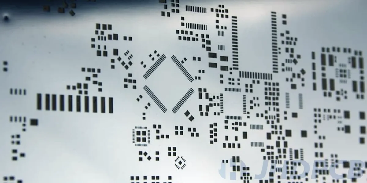
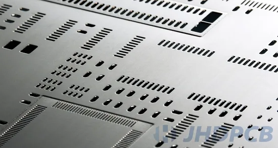
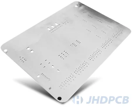
PCB stencils are thin sheets of stainless steel with precisely cut apertures using laser technology, which are intended to apply solder paste on a circuit board for mounting surface-mounted components. Stencil types may vary based on their aperture type and mounting style:

  • Laser-cut Stencils: Laser-cut stencils are a high-precision type of solder paste stencil used in PCB assembly, created using a laser beam to cut openings in a stainless steel sheet. They offer precise control over aperture size and shape, making them ideal for small pad sizes, fine-pitch components, and complex designs. Laser-cut stencils are durable, compatible with both manual and automated processes, and provide flexibility in production methods. Overall, they are an excellent choice for high-precision PCB assembly, offering accuracy, durability, and flexibility.

    Laser-cut Stencils

  • Chemical-etch Stencils: Chemical-etch PCB Stencils are made by using acid to etch openings into metal. While these stencils are inexpensive and manufactured quickly, the chemicals involved in the production process can be detrimental to the environment.
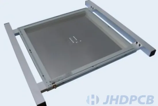
  • Framed / Framework PCB Stencils: Stencil frames are typically made of a mesh border and are utilized to maintain the stencil sheet’s tautness for better accuracy in “PCB stencils”. Framed PCB stencils are the preferred choice for large-scale PCB production because of their dependable repeatability and superior print quality.

    Framed&Framework PCB Stencils

  • Frameless/ Reusable PCB Stencils: PCB stencils without frames, also known as reusable PCB stencils, are a cost-effective and versatile option for applying solder paste in PCB assembly. They can be easily adjusted to fit different board sizes, and are typically less expensive than stencils with frames. They work well with both automated and manual assembly processes, making them useful for small-scale prototyping and hand-soldering applications. In addition, frameless/reusable PCB stencils take up less storage space than traditional stencils. However, they may require careful handling during the printing process to ensure accurate solder paste placement. Overall, frameless/reusable stencils provide valuable accuracy and precision for PCB designers and manufacturers.

    Frameless&Reusable PCB Stencils

  • Prototype PCB or Photo Stencils: Prototype/photo stencils are custom-made based on specific design requirements using CAD/Gerber files and made through photolithography. They offer high precision and accuracy for manual printing and prototyping with small batch sizes and quick turnaround times. Nonetheless, they are costly, delicate, and not cost-effective for larger runs, yet crucial in fine-tuning PCB designs before mass production.
  • Hybrid PCB Stencils: Hybrid PCB stencils are highly precise and accurate solder paste stencils used in the assembly of PCBs. They are made using a combination of chemically etched and laser-cut techniques, providing high accuracy in fine details and flexibility in customized shapes. Hybrid stencils are useful for small pad sizes and complex designs, with materials such as stainless steel and nickel ensuring durability for multiple assembly uses without degradation in quality.

Structure of PCB solder paste stencil.

Stencil Holder: The stencil holder can be classified into a movable holder and a fixed holder. The movable holder directly fastens the steel sheet onto the holder, and one stencil holder can be reused multiple times. The fixed holder uses adhesive to attach the wire mesh to the stencil holder, providing uniform tension with a range of 35 to 48N/cm2 (normally fixed holders allow for 35N-42N).

Mesh: Mesh serves as a means to secure the steel sheet to the stencil holder. It can be categorized as either stainless steel mesh or polymer polyester mesh. Stainless steel wire mesh is typically around 100 mesh, providing stable and adequate tension, but is prone to deformation and loss of tension over time. Polyester mesh does not deform easily and has excellent durability.

Sheet: Steel sheets can be made of copper, stainless steel, nickel alloys, polyester, etc. Stencils typically use high-quality 301/304 stainless steel sheets, which significantly improve the stencil’s service life with their excellent mechanical properties.

Adhesive: The choice of adhesive for attaching the mesh frame to the steel sheet is a critical factor in stencil production. It can be selected based on the customer’s requirements, maintaining strong adhesion and resistance against various stencil cleaning agents.

What are the production methods of PCB stencil?

JHDPCB is an experienced manufacturer of PCB, offering a range of PCB stencils production methods such as laser cutting, chemical etching, and electroforming. Our state-of-the-art equipment and advanced technology ensure that our stencils are precise, reliable, and suitable for a wide range of applications. We have a team of skilled engineers who can assist with stencil design and manufacturing, providing guidance on factors such as aperture size and placement, as well as fiducial mark placement and stencil thickness. We provide tailored solutions, including bonding stencils and step stencils, to fulfill our customers’ unique needs.
Here is a more detailed explanation of the different methods for manufacturing PCB stencils:

This process involves applying a resist material to the metal surface of the stencil and then etching away the unwanted areas with a chemical solution. Although this method is cost-effective and straightforward, it may not be ideal for intricate or delicate designs.

Process:

  • The metal surface of the stencil is covered with a resist material that is impervious to the chemical etchant.
  • A pattern or design is created on the resist material, using various techniques such as photolithography or screen printing.
  • the stencil is submerged in an etchant that removes the metal from the exposed areas not protected by the resist material.
  • Once the etching process is complete, the resist material is stripped away, revealing the desired pattern on the metal stencil.

Characteristics:

  • Chemical etching is a flexible and versatile method that can be used to create stencils with a wide range of shapes and sizes.
  • This process is straightforward and economical, and only requires basic equipment.
  • Chemical etching can achieve high tolerances and precision for certain designs, but may not be suitable for more complex patterns.
  • The resulting stencils have a high level of detail and sharp edges.
  • Chemical etched stencils are typically made from thin sheets of metal, which can be easily bent or warped during handling and storage.
  • The process is eco-friendly since it doesn’t generate any hazardous byproducts or waste.

The creation of “laser cut stencils” involves the use of a powerful laser to accurately form openings in the stencil material. This method is the most widely utilized for manufacturing pcb SMT stencils owing to its high precision, speed, and design versatility.
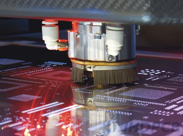
Laser cutting

Process:

  • The stencil material is mounted onto a cutting bed.
  • A CAD file or other digital design is loaded into the laser cutting system.
  • The laser beam follows the design, cutting precise apertures into the stencil material, creating the desired pattern.
  • Once the cutting procedure has finished, the stencil is taken out from the cutting platform.

Characteristics:

  • Laser cutting is a highly accurate and precise method of stencil manufacturing.
  • It can create very small, intricate designs with tight tolerances.
  • This method is fast and efficient, allowing for high-volume production.
  • Laser cutting is a flexible process that can be used with a variety of stencil materials.
  • This method may be more expensive than other methods, but is often preferred due to its high level of precision.

This process involves depositing metal onto a mandrel or substrate to create a reverse image of the desired pattern. Afterward, the metal layer is detached from the cylindrical shaft to produce the stencil. This method is capable of producing very fine and complex designs, but is generally more expensive than other methods.

Process:

  • A cylindrical shaft or base is fabricated with the inverted design of the intended pattern.
  • The base is subsequently covered with a conductive coating, such as copper.
  • The substrate is immersed in an electrolytic solution, causing metal ions to deposit onto the conductive layer, gradually building up the stencil in the desired pattern.
  • Once the desired thickness is reached, the stencil is removed from the mandrel or substrate.

Characteristics:

  • Electroforming can create extremely fine and complex patterns with high precision.
  • This method allows for tight tolerances and fine details.
  • Stencils produced through electroforming are extremely robust and have the ability to endure frequent usage.
  • This technique may incur higher costs compared to other alternatives, primarily due to its intricacy.

These are specialized stencils that have multiple levels or steps, allowing for the use of different solder paste volumes for different component sizes or types.

Process:

  • A stencil is created with multiple levels or steps, each with a different aperture size.
  • The solder paste is applied to each step based on the component size or type.
  • The stencil is carefully aligned to ensure accurate paste placement.
  • The excess paste is scraped off the surface of the stencil, leaving behind only the paste required for each step of the process.

Characteristics:

  • Step stencils allow for precise solder paste application, ensuring consistent placement and reducing the likelihood of bridging or other defects.
  • They are typically used in applications where different component sizes or types require different paste volumes.
  • Step stencils can increase production efficiency and reduce waste materials.

These stencils are made by bonding a thin foil to a metal frame. This can provide increased durability and rigidity for stencils that will be used repeatedly.

Process:

  • A thin foil is bonded to a metal frame to create a more durable and rigid stencil.
  • The stencil aperture pattern is created using one of the other stencil manufacturing methods, such as laser cutting or chemical etching.
  • The stencil is then mounted onto the frame for use.

Characteristics:

  • Stencils that utilize bonding techniques are longer-lasting and have the ability to endure frequent usage.
  • They are often preferred in high-volume production environments where stencils need to be used multiple times.
  • This method can increase stencil rigidity, which can improve accuracy and reduce defects.

This method involves coating a stainless steel stencil with nickel to improve its durability and resistance to wear.

Process:

  • A stainless steel stencil is coated with a layer of nickel.
  • The nickel coating increases the durability and wear resistance of the stencil.
  • The stencil aperture pattern is created using one of the other methods, such as laser cutting or chemical etching.

Characteristics:

  • Nickel plating stencils are highly durable and can withstand repeated use.
  • They offer increased wear resistance.
  • This method is often preferred in high-volume production environments.
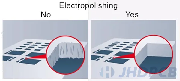
This process uses an electrolytic solution to remove surface irregularities and improve the flatness of the stencil material. This can improve the consistency of solder paste application, but may not be necessary for all applications.
In terms of SMT stencils, laser cutting is generally the preferred method due to its precision, speed, and flexibility in terms of design. The data file required for laser cutting must contain the SMT solder paste layer, fiducial mark data, PCB outline layer, and character layer to ensure accurate production. Stencils can be checked for details such as the front and back sides of the data, component categories, etc. to ensure optimal performance during assembly.

Electropolishing stencil

Process:

  • A stencil is fabricated using a standard manufacturing process.
  • The stencil is immersed in an electrolyte solution and placed in an electrochemical cell.
  • A DC current is applied to the stencil, causing metal ions to dissolve from the surface of the stencil.
  • The dissolved metal ions are removed from the surface of the stencil, leaving behind a smooth and polished surface.

Characteristics:

  • Improved paste release: Electropolishing removes any roughness or burrs on the stencil surface, which improves paste release and reduces bridging and other defects.
  • Increased stencil lifespan: Electropolishing can extend the lifespan of stencils by removing any rust, corrosion, or damage that may have occurred during previous use.
  • Consistent aperture size and shape: Electropolishing can ensure consistent aperture size and shape across the entire stencil surface, which helps to improve the accuracy and consistency of paste placement.
  • Cost-effective: Electropolishing can be a cost-effective way to rejuvenate stencils and extend their lifespan, reducing the need for frequent stencil replacement.
  • Environmentally friendly: Electropolishing is an eco-friendly procedure, since it does not demand the use of harsh chemicals or create hazardous waste materials.

What are the basic requirements for PCB stencil?

There are several basic requirements that a PCB stencil must meet in order to ensure accurate, consistent and reliable SMT solder paste application during PCB assembly. These stencil requirements include:

  • Proper aperture size and shape: The stencil must accurately transfer the correct amount of solder paste onto each pad of the PCB, so the aperture size and shape must be precisely matched to the component pad dimensions.The aperture size should generally be 5-10% larger than the component pad size to ensure sufficient solder paste coverage. For example, if a component pad is 1mm x 1mm, the aperture size might be 1.05mm x 1.05mm to 1.1mm x 1.1mm. The aperture shape may vary depending on the specific component pad shape, but is often rectangular or square.
  • Accurate aperture placement: The apertures must be placed with high precision relative to the PCB pads to ensure that the correct solder volume is applied to each pad.The aperture placement must typically be accurate within +/- 0.025mm. For example, if the center of a component pad is at position (X=10mm, Y=10mm), the center of the corresponding aperture should be at position (X=10mm +/- 0.025mm, Y=10mm +/- 0.025mm).
  • Adequate thickness: The stencil must be thick enough to maintain its structural integrity and withstand repeated use, but not so thick as to interfere with the proper transfer of solder paste.The thickness of the stencil typically ranges from 0.1mm to 0.2mm, depending on the specific manufacturing process and component requirements. A common value is 0.127mm (5 mils).
  • Consistent and smooth aperture walls: The walls of the apertures must be uniform in thickness and free from any burrs, scratches or other defects that could affect the quality of transfer.The walls of the apertures should be uniform in thickness, with typical tolerances of +/- 0.0127mm.
  • Fiducial mark alignment: The stencil must have fiducial marks that match those on the PCB to ensure accurate alignment during assembly.The fiducial marks should typically have a diameter of 1mm and be positioned with an accuracy of +/- 0.025mm relative to the PCB pads.
  • Compatibility with assembly equipment: The stencil must be compatible with the specific pick-and-place machines and reflow ovens used in the assembly process. See the difference between reflow and wave soldering.

Meeting these basic requirements is essential for ensuring successful PCB assembly with reliable and consistent solder paste application.Working with a professional PCB template manufacturer like JHDPCB to understand the importance of these requirements can help ensure that the final product meets all necessary specifications and performs optimally during assembly.

PCB Solder Paste Stencil Design Guidelines.

  1. Pad shape and size: The pad size and shape for SMD components can be determined using IPC standards as a guide. For example, the recommended pad size for a 0805 component is 80mm x 1.25mm.
  2. Aperture size and shape:The aperture size and shape should match the pad size and shape. As a general rule of thumb, the aperture size should be around 2-4 mils larger than the pad size to allow for proper paste deposition.
  3. Stencil thickness: The stencil thickness is generally between 4-7 milsdepending on the size of the aperture. Thicker stencils may be required for larger apertures, while thinner stencils can be used for smaller apertures.
  4. Opening ratio:The opening ratio should be optimized for each pad size and shape. For example, a 8mm x 1.25mm pad for an 0805 component with a 5-mil stencil thickness might have an opening ratio of around 60-70%. The opening ratio will affect the amount of paste deposited on the pad, with higher opening ratios resulting in more paste transfer.
  5. Fiducial marks:Fiducial marks should be placed carefully to ensure accurate alignment between the stencil and the PCB. As a guideline, consider using 1mm round fiducial marks located diagonally from each other at a distance of at least 10mm.
  6. Alignment marks: Alignment marks can be used to ensure correct orientation during stencil application. For example, if using a Mylar stencil, consider placing a cross mark in the middle of the stencil.
  7. Rounding edges:Rounding the edges of the stencil apertures can improve paste transfer and reduce bridging between pads. A common rounding value is around25mm.
  8. Solder paste type:The type of solder paste being used should be considered in the design process. Different paste types have different viscosity and require different stencil design parameters. For example, a thinner paste will require a smaller aperture opening ratio compared to a thicker paste.
  9. PCB Layout: The PCB layout should be considered in the stencil design process. This includes the orientation of the components, the spacing between the pads, and the overall board dimensions. Consider using a centered stencil for optimum alignment with the PCB.
Recommended Aperture Parameters for Common Package Types
Component PackageRecommended Aperture Parameters
0805– Cut two pads of the opening by 1.0mm.
– Make a concave circle with B = 2 / 5Y and A = 0.25mm or a = 2 / 5 * l anti-tin bead
Chip 1206 and above– Move two pads outward by 0.1mm.
– Make an inner concave circle with B = 2 / 5Y and A = 2 / 5 * l anti-tin bead
BGA– Ball spacing > 1.0mm: opening ratio 1:1.
– Ball spacing < 0.5mm: opening ratio 1:0.95
QFP and SOP– 0.5mm pitch: opening ratio in total width direction 1:0.8.
– Length direction: opening ratio 1:1.1.
– 0.4mm pitch QFP: opening in total width direction 1:0.8, opening in length direction 1:1.1, outer rounding foot chamfer radius r = 0.12mm.
– 0.65mm pitch SOP: reduce total opening width by 10%
PLCC32 and PLCC44– General products: total width direction 1:1, length direction 1:1.1
SOT packaged devices– Small pad end: opening ratio in total width direction 1:1, length direction 1:1

How to purchase PCB stencil?

When selecting a PCB stencil that meets all of your needs, it is important to consider the following key points:

  • Thickness of the stainless steel sheet.
    The precise thickness of the stencil sheet is critical to ensuring the proper expulsion of solder paste from the aperture. Board thickness and aperture size are key factors that can impact the amount of solder paste applied to the board, as excessive solder deposits can cause solder bridging, while insufficient coverage can result in weak solder joints that compromise the functionality of the finished PCB.
  • Size of the aperture opening.
    To avoid prevalent soldering defects, such as bridging and solder balls, the aperture opening should be marginally smaller than the size of the PCB pad. After soldering, the solder paste may stick to the walls of the stencil opening or migrate to the board if the PCB pad area is less than two-thirds of the area inside the stencil hole wall.
  • Stencil Material.
    The choice of stencil material can also affect the transfer of solder paste from the apertures to the PCB pads. Typically, stainless steel is used for stencil production, though other nickel-based materials may also be employed.
  • Stencil Alignment.
    To facilitate the accurate application of solder paste onto the PCB pads, fiducial marks are incorporated onto both the PCB and stencil. These registration marks guarantee alignment between the circuit board and the stencil, which is essential in preventing negative impacts on device function caused by surface-mounted parts being out of alignment. As a result, stencil alignment prior to paste application is critical.

How to use PCB solder paste stencil?

Using PCB Solder Paste Stencils

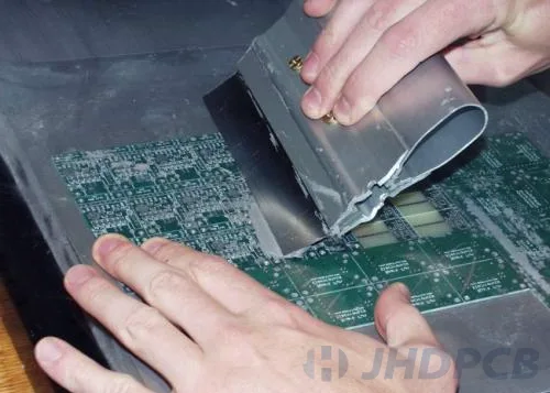
Positioning is a crucial step when using a solder paste stencil to avoid errors and ensure proper alignment of the stencil on the PCB. Below are the procedures for correctly positioning a stencil for applying solder paste to a PCB:

  1. Place the PCB: The first step is to place the PCB in a fixture or clamp to make sure it’s securely held in place.
  2. Stencil alignment: Align the stencil over the PCB to match the pads on the board with the holes in the stencil. An alignment tool can be employed to ensure precise stencil alignment.
  3. Fix the stencil: Once the stencil is aligned correctly, fix it in place on the PCB using a vacuum table or other holding mechanisms that will prevent it from moving while applying the paste.
  4. Apply the solder paste: Using a squeegee or scraper, apply the solder paste evenly over the stencil, covering all the holes for the pads. It’s crucial to apply the paste gently and smoothly without leaving gaps or excess paste on the stencil.
  5. Inspect the results: After applying the paste, carefully lift the stencil away from the PCB and inspect the pads to make sure each pad has been covered with an even layer of paste.PCB stencil kits can be used to accurately apply solder paste to the printed circuit board during assembly.
  6. Remove excess paste: If there is any excess paste on the pads, clean it off using a lint-free cloth or other suitable material. Any missing paste must be carefully applied manually to ensure proper coverage of the solder pads.

By following these steps, you can position the PCB stencil correctly, which will ensure proper alignment and consistent paste application, resulting in high-quality solder joints and a successful PCB assembly.

Symptoms and countermeasures of insufficient solder paste.

A good solder paste printing shape should be uniform in both the horizontal and vertical directions, with a smooth and full appearance that fully covers the pads and has clean edges. When this type of pattern is printed onto components and subjected to reflow soldering, a good solder joint should form. However, if the solder paste printing process is done improperly, it can lead to poor printing results that fail to meet these standards.

  • Causes: Improper alignment of the stencil plate or deviation from the pad location; Lack of accuracy in the printing machine.
  • Hazard: Possible occurrence of solder bridging.
  • Countermeasures: Adjust the stencil plate position; Adjust the printing machine settings.
  • Causes: Excessive pressure from the scraper; Insufficient hardness of the rubber scraper; Improper design of stencil window.
  • Harm: Insufficient solder, resulting in weak solder joints and possible open circuits.
  • Countermeasures: Adjust printing pressure; Change to a metal scraper; Improve stencil window design.
  • Cause: Large stencil window size; Large clearance between stencil plate and PCB.
  • Harm: Possible occurrence of solder bridging.
  • Countermeasures: Check stencil window size; Adjust printing parameters, particularly stencil plate clearance.
  • Causes: Poor quality stencil window walls; Inadequate removal of residual solder paste after multiple printings; Poor thixotropic properties of the solder paste.
  • Harm: Possible occurrence of inadequate solder, leading to poor solder connections that can result in open circuits or other defects.
  • Solution: Clean the stencil; Ensure proper printing parameters for optimal thixotropic behavior.
  • Causes: Multiple printings without sufficient cleaning of the stencil; Poor quality of the solder paste; Vibration of the stencil plate during printing.
  • Harm: Possible occurrence of solder bridging.
  • Countermeasures: Clean the stencil thoroughly; Adjust the printing machine parameters and use a high-quality solder paste.
  • Causes: improper preparation and management of the bath solution, incorrect formulation, or untimely replenishment of components in the bath solution, insufficient or unbalanced current density and plating time.
  • Hazards: poor adhesion, uneven coating thickness, and reduced resistance.
  • Countermeasures: adjust and maintain the composition of the bath solution regularly, increase the current density and prolong the electroplating time to ensure uniform coating thickness.
  • Causes: improper design of the anode plate, oxidation of the anode plate, or insufficient anode maintenance.
  • Hazards: uneven coating thickness and poor surface finish.
  • Countermeasures: Possible measures include conducting random checks on anode consumption, incorporating anodes with appropriate consumption levels, optimizing the distribution of anodes, decreasing current density, and rationally designing the wiring or splicing board.
  • Causes: improper composition of the polish, excessive or insufficient use of polish, or inappropriate polishing temperature.
  • Hazards: Low-quality surface appearance and inconsistent layer depth.
  • Countermeasures: Hirschner trough analysis to adjust the content of light agent, and adjust the amount of polish for optimum surface finish.
  • Causes: improper design of current density, wire density, or light agent balance, or insufficient anode maintenance.
  • Hazards: uneven coating thickness and poor surface finish.
  • Countermeasures: adjust the design of current density, wire density, or light agent balance, reduce the current density, and optimize the anode maintenance.
  • Causes: inadequate pretreatment of the surface before plating, improper cleaning, or insufficient rinsing.
  • Hazards: poor adhesion and uneven coating thickness.
  • Countermeasures: reinforce the pretreatment of the surface before plating, use proper cleaning and rinsing procedures, and improve the storage process.
  • Causes: insufficient filtration of the plating bath, improper maintenance, or an incorrect design of the filtration system.
  • Hazards: uneven coating thickness and poor surface finish.
  • Countermeasures: Preventive actions could include routinely servicing or degrading the filter system and closely regulating the storage duration and environmental circumstances during storage.

In summary, achieving an excellent solder paste printing shape is crucial for obtaining a good welding effect. However, there are many factors that can lead to a bad printing effect, such as solder paste dislocation, drawing points and depressions, too much or non-uniform solder paste quantity, figure stain, and others. As a result, it is crucial to implement remedial measures such as fine-tuning printing parameters and performing routine equipment maintenance. Similarly, proper plating procedures and maintenance are essential to prevent uneven coating thickness, poor surface finish, and other hazards caused by factors such as improper bath solution composition, anode design, or insufficient pretreatment. By following the correct procedures and taking care of the equipment, high-quality products can be consistently obtained.

How to clean PCB stencil?

  • Remove excess solder paste: Once the PCB stencil has been used, any excess solder paste should be carefully removed from the stencil using a spatula or scraper. The excess paste should be collected and disposed of safely.
  • Solvent cleaning: To clean the stencil, a suitable solvent for the stencil material should be used after the excess paste has been removed. Isopropyl alcohol and acetone are commonly used solvents for stencil cleaning. A clean, lint-free cloth or sponge can be used to apply the solvent.The solvent helps to dissolve any remaining paste residue and other contaminants on the stencil surface.
  • Rinse with water: After cleaning the stencil with a suitable solvent, it is necessary to rinse it thoroughly with water to eliminate any remaining debris or solvent. It is important to exercise caution to prevent the bending or any harm to the stencil while carrying out the rinsing procedure. It is crucial to ensure that there is no residual solvent left before proceeding to the next step.
  • Stencil drying: Once rinsed, the stencil should be dried completely using either compressed air or a clean, lint-free cloth while taking care not to cause any damage or distortion. The stencil must be absolutely dry before reuse to prevent any moisture residue from interfering with paste application.
  • Defect inspection: Following cleaning and drying, it is critical to examine the PCB stencil for debris or defects that could potentially compromise the solder paste application quality. Any found debris or defects must be remedied before stencil reuse. This inspection assures accurate and consistent paste application.

By following these steps, you can keep your PCB stencils clean and in good condition, contributing to higher-quality soldering and better performance of the electronic products they are used in.

PCB stencils play a critical role in the PCB manufacturing process. With an accurately positioned stencil, the solder paste can be applied precisely and consistently, which is essential for delivering high-quality electronic products. As a professional PCB manufacturer, JHDPCB has advanced technologies and equipment to produce high-quality PCB stencils and printed circuit boards that meet the diverse needs of customers.Our dedication is to furnish clients with the most exceptional services and products to support them in accomplishing their objectives. With a reputation for reliability, JHDPCB is the ideal choice for those seeking a trustworthy PCB manufacturer.

Get a PCB Quote Now

Open high-quality PCB manufacturing services in JHDPCB

Leave a Comment