PCB ground plane

The role and design guidelines of PCB ground plane.

directory

In the intricate world of Printed Circuit Boards (PCBs), the ground plane plays a vital role in ensuring the reliable and efficient operation of electronic devices. As a leading PCB manufacturer, JHDPCB understands the significance of the ground plane and its impact on the overall performance of circuits. In this article, we delve into the essential aspects of the PCB ground plane, demystifying its purpose and benefits.

Understanding the ground plane is crucial for designers and engineers to create high-performance PCBs. Our comprehensive guide will explore the importance of proper ground plane design, its impact on signal integrity, and techniques for optimizing its functionality. Trust JHDPCB’s expertise in PCB manufacturing as we provide valuable insights into the world of ground planes, helping you design and implement PCBs that meet the highest standards of quality and performance.

What is a PCB ground plane?

A ground plane PCB refers to a crucial element in the construction of a printed circuit board. It is essentially a dedicated metal layer, often composed of copper foil, that is strategically placed within the board’s stack-up. By connecting directly to the circuit’s ground, which is typically linked to the power supply’s negative terminal, the ground plane serves multiple important purposes.
First and foremost, the groundplane acts as a return path for the majority of components and electrical currents in the circuit. It provides a low-impedance pathway for the flow of current, enabling efficient and reliable operation of the electronic devices. This helps to minimize voltage fluctuations and ensures that signals propagate smoothly throughout the PCB.
Beyond its role as a conductive pathway, the ground plane also serves as a shield, effectively mitigating various types of undesirable electrical noise and interference. By surrounding the circuitry with a contiguous conductive surface, it helps to suppress and divert unwanted electromagnetic radiation that may arise from both internal and external sources. This shielding effect significantly reduces the likelihood of signal cross-talk and minimizes the potential for electromagnetic interference (EMI) between different components on the PCB.

The positioning and allocation of the ground plane within the PCB design can vary depending on the board’s complexity and layer configuration. In a two-layered PCB, the ground plane is typically allocated to the bottom layer. However, in multi-layered boards, the entire layer is dedicated to grounding to ensure the avoidance of ground loops, signal trace interference, and other related issues.

Multi layer PCB-FR4-4 layers-lead free hasl-smart home-3-PTH

It is crucial to carefully determine the appropriate ground plane technique for a given PCB design to achieve optimal results. Choosing an unsuitable ground plane configuration can lead to a host of problems. For instance, improper grounding may result in signal crossroads, where signals inadvertently interfere with one another, leading to data corruption or erratic behavior. Additionally, without a well-designed ground plane, the PCB may be more susceptible to electromagnetic interference generated by other components, further degrading the performance and reliability of the circuit.
In summary, the PCB ground plane plays a vital role in the overall functionality and performance of electronic circuits. Acting as a reliable return path, noise shield, and interference suppressor, it ensures proper signal integrity and mitigates the risks associated with unwanted electrical noise. Although the ground plane occupies a relatively small portion of the board’s physical area, its impact on the successful operation of the PCB is immense.

What are the different nodes on the PCB ground plane?

There are several nodes or areas on the PCB ground plane that serve a specific purpose; common nodes on the PCB ground plane are described below. There are several types of nodes called grounds, including floating ground, virtual ground, AC ground, earth ground, and chassis ground.

  • Floating grounds: This node is a reference point in the system that is not physically connected to the mass and is isolated.
  • Virtual grounds: This node is located in the negative feedback loop of the inverting terminal of the operational amplifier. When the non-inverting input is zero volts, the feedback causes the inverting terminal to correspond to this value in a stable circuit. This value is maintained only by feedback, as no other circuit can provide stable feedback.
  • AC Grounds: This node has a low impedance dc value. This dc voltage is stable in the presence of small disturbances. Because of its DC value, this node cannot be used as an exact ground, but it is stable and can be used as a reference point.
  • Chassis grounds: In large electrical systems, earthing literally means connection to the earth. For example, every house has copper stakes driven into the earth to dissipate excess current.
  • Power Supply Grounds: While the electronic circuitry on a circuit board cannot be connected to a physical ground, case grounding serves the same purpose. This ground is the connection for the safety cable that connects from the AC power source to the product’s enclosure or chassis.
    It is the ground of the power supply: this node is connected to the power supply ground terminal and serves as a reference point for the entire circuit. This ensures that all components have the same ground potential and provides a stable voltage reference for the circuit.
  • Component Ground Nodes: These nodes are connected to the ground pins of individual components on the PCB. They serve as local reference points for specific components, allowing them to establish their own ground reference and minimizing the interference they may cause to other parts of the circuit.
  • Analog Ground Node: In circuits that involve analog signals, an analog ground node is used to isolate the analog components and their associated signals from digital noise. This helps to maintain signal integrity and reduce unwanted noise coupling between analog and digital sections of the PCB.
  • Digital Ground Node: Similar to the analog ground node, the digital ground node is used to provide a separate ground reference for digital components and signals. It helps prevent digital noise generated by high-speed switching logic from interfering with sensitive analog components.
  • RF Ground Node: In RF (Radio Frequency) circuits, a dedicated RF ground node is used to establish a low-impedance path for RF signals and minimize RF interference. This node is carefully designed to reduce the parasitic effects and maintain signal integrity at high frequencies.
  • Chassis Ground Node: In certain cases, a PCB may be connected to a chassis or enclosure for grounding and mechanical stability. The chassis ground node establishes a connection between the PCB and the grounding structure of the system, ensuring proper grounding and providing a safe discharge path for any electrical faults.

Because an earth ground and chassis ground serve the same function, these terms are often used interchangeably along with the term safety ground. Click to learn more about PCB terminology. These nodes, along with their interconnections, help to create a well-structured and efficient grounding system on the PCB. By carefully designing and separating these nodes, the risk of ground loops, signal interference, and noise coupling can be minimized, resulting in improved circuit performance and reliability.
There is no universal method for grounding printed circuit boards. To determine the best method for grounding a system, it is necessary to understand the current flow within the system. However, there are a variety of methods to choose from, and there are suggestions for the best grounding method that apply to most systems. To determine the best method for your board, you will need to familiarize yourself with the board design and possibly try different pcb grounding techniques.

What is the role of the ground plane on a PCB?

As already mentioned, the PCB ground plane is a particularly large part that is usually made of metal and is connected to the PCB ground. This area does not have a fixed structure. Instead, it depends entirely on the requirements of the circuit. Therefore, the metal part can sometimes be a small part of the entire PCB, and sometimes it can become a huge insert if the PCB design contains many inserts.

  • Voltage recovery: A PCB contains numerous components that are connected to power nets for operation. The return current from these components typically flows through the ground net. The ground plane provides a low-impedance path for the return current to flow, ensuring efficient voltage recovery and minimizing voltage drops or fluctuations.
    A multilayer PCB design with more than four layers requires more attention, so the manufacturer should use a high-quality board for the ground plane. The goal is to ensure a reliable connection between grounding networks and circuit components.
  • Signal recovery: The ground plane helps maintain signal integrity by providing a reference point for signals on the PCB. It acts as a stable and consistent voltage reference, reducing noise and interference that could affect signal quality. By providing a solid ground reference, the ground plane helps ensure accurate and reliable signal transmission.
  • Reduction of noise and interference: As the signal speed increases, more and more digital circuits change state. This causes noise pulses in the ground plane that can affect other parts of the circuit. A ground plane with a large conductive area helps reduce this noise because it has a lower impedance than the ground network running through a path.
  • EMI Shielding: The ground plane acts as a shield, providing electromagnetic interference (EMI) protection for the PCB. It helps contain and prevent the propagation of unwanted electromagnetic signals that could interfere with the proper functioning of the circuit. The large metal area of the ground plane absorbs and dissipates EMI, reducing the risk of cross-talk and improving the overall electromagnetic compatibility (EMC) of the PCB.
  • Heat Dissipation: The ground plane helps with heat dissipation in the PCB. It acts as a large conducting area that can absorb and spread heat generated by active components or high-power components. By providing a thermal pathway, the ground plane helps dissipate heat and prevent localized hotspots, ensuring the reliability and longevity of the circuit.
  • Reduced Impedance: The ground plane offers a low-impedance path for current flow, reducing the resistance and inductance in the circuit. This helps improve the efficiency and performance of the circuit by minimizing voltage drops and maintaining stable power distribution.
  • Ease of Routing: The ground plane simplifies the routing of traces and connections on the PCB. It provides a common reference point and serves as a convenient return path for signals and currents. By reducing the complexity of routing, the ground plane facilitates easier and more efficient PCB layout, enhancing the overall manufacturability and reliability of the circuit.
  • Power supply integrity: nted circuit boards often contain electronic components that require high power during their operation. Therefore, PCB ground planes attenuate the power spikes created by this operation.

In addition to the above functions, the ground plane also has other functions. These roles are as follows.

  • Distributes direct current to active devices.
  • The grounding plane eliminates crosstalk between signals.
  • It distinguishes between the analog and digital parts of the PCB.
  • It has a huge capacity to transfer energy.
  • It can dissipate the heat in electronic devices.

In summary, the PCB ground plane performs functions such as voltage recovery, signal integrity, EMI shielding, heat dissipation, impedance reduction and simple routing. Its presence is critical for proper grounding, minimizing noise and interference, improving thermal management, and increasing overall board performance and reliability.EMI shielding, heat dissipation, reduced impedance, and ease of routing. Its presence is essential for ensuring proper grounding, minimizing noise and interference, improving thermal management, and enhancing the overall performance and reliability of the printed circuit board.

Use design tools to effectively design PCB Ground plane.

The key to creating a good ground plan for your PCB design is to let the tools do the work. Make sure you have established all design rules and constraints before you begin working with layers. Most PCB CAD systems allow you to set different connection parameters for different networks and layers to be connected. In addition, the rules and constraints of the PCB design system provide great flexibility in setting distances. This is also helpful when creating bulk plans, as the tool does all the work, so you only need to specify where to place the plan.

Until a few years ago, all PCBs had more or less the same format. Each PCB had a six-layer layout, with a basic ground plane and VCC plane. Traditional CAD techniques focused on the VCC plane rather than the power plane. With modern CAD strategies, it is possible to customize the PCB to create the desired ground plane. Before that can be done, however, the following steps must be taken.

  • Analyze whether the grid on the PCB is correct:
    Before proceeding, it is necessary to verify that the schematic grid of the created ground plane or power plane is valid. If the layout does not follow the PCB layout rules for ground planes, the result will only be a big zero.
  • Always use internal planes when creating ground planes:
    If you want to get the best results, using internal planes when designing ground planes is a prerequisite. The choice between negative and positive internal planes is up to you.
  • Use polygonal infill:
    If you prefer to build positive ground planes, this system or tool is perfect for you.
    Another thing that helps when working with layers is to first make sure that the layers of the board are completely set up. That way, you don’t have to worry about changing the layout or shape of the layers during the design process, since the layout of the layers is already set. To take full advantage of the features described, you need to work with a PCB design tool that can create ground planes.
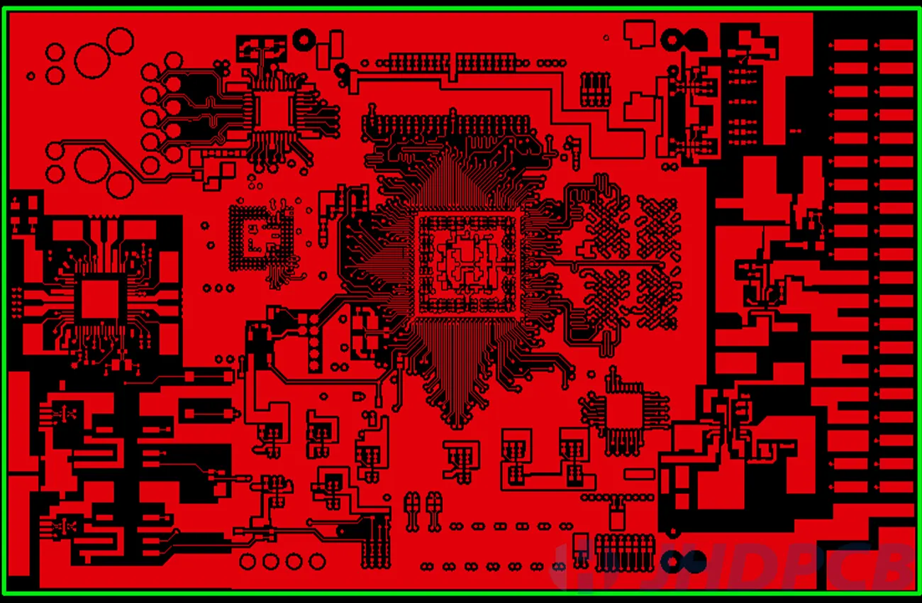
    The following figure shows a typical multilayer PCB used for a 4-layer PCB. The ground plane is on the inner layer, next to the power layer. The top and bottom layers are signal layers, providing ample space for components and routing.

    pcb stackup

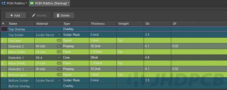
Keeping these details in mind, you can choose whichever tool seems a good fit for your model. However, for getting a considerable outcome, follow the PCB ground plane rules thoroughly.

Printed Circuit Board Ground Plane Design Guidelines.

Layouts can be created using PCB design tools. However, when it comes to PCB multiple ground planes, it’s important to follow the layout rules. When it comes to multilayer pcb power ground planes in PCB design, there are a few layout rules that will help you create the most reliable ground system possible:

On single-layer PCBs, wiring should be routed as widely as possible if it’s not possible to fill the area. However, it is preferable to create a form of ground plane wherever possible in order to take advantage of the electrical benefits described above in all other designs.

In high-speed multilayer designs, the PCB layer structure must be calculated to correctly configure the ground plane, dielectric materials and layer widths required for impedance control routing. The ground plane itself can be created as a positive or negative image in the CAD system, depending on what best suits the CAD system and the manufacturer. In many cases, it is necessary to fill in the ground plane area throughout the design. Some designs may require separation of ground planes, but this should be avoided wherever possible for reasons of signal integrity.

The paths between SMT pads and ground holes should be wider to reduce inductance. At the same time, care must be taken with small discrete components, as too wide a routing can lead to thermal imbalance and potential production problems. For through-holes, thermal breaks should be used to ensure a good solder connection. In addition, small grounding holes can usually be replaced by solid terminals.
To create a production-ready PCB, layout teams need to follow a number of design rules, but fortunately, CAD tools can meet these requirements.

Make sure there’s nothing unnecessary in the PCB layout. It’s a good idea to fill any empty space with copper to create holes that connect to the ground plane. This will provide a structural path for all signals to actually reach ground.

If you have a dedicated ground plane, as is the case with many four-layer PCBs, make sure there is no root path. Separating and routing the grounding layer will result in pcb ground loop. Eliminate the grounding layer completely.

Every PCB must have a single point where all grounds meet. This is often the metal frame or chassis of the product. It can also be a specific layer of the board. This single point is often referred to as a “star ground”, as the various conductors start from this point in a pattern that somewhat resembles a star. In mixed-signal applications, there may be separate analog and digital power supplies that have separate analog and digital grounds that meet at the star point.

It’s best to minimize the number of vias along your ground paths and send component grounds as directly as possible to the ground plane. Adding more vias to a board creates additional impedance. This consideration is particularly crucial for fast transient currents, which can cause an impedance path to become a voltage differential.

Grounding must be designed prior to routing. Ground is the foundation of the routing process, so it’s crucial to design it correctly. If a ground is poorly designed, the whole device is at risk, whereas this is not the case if a single signal doesn’t work as intended.

Understanding where currents flow on a board can help ensure correct grounding. It’s essential to consider the destination of the signal, as well as the return path it will take. The transmit and return paths of a signal have the same current, which can have an impact on ground bounce and power supply stability.

In a multi-board system, it’s important to allow for dynamic variance when sending ground connections between boards. This is particularly important for applications requiring long-distance cables. Optical isolators, low-voltage differential signals and common-mode chokes.

If analog and digital signals are to be processed simultaneously, care must be taken in design. The analog parts of the board, including the analog-to-digital converter (ADC) and DAC, must be isolated; the ADC ground can be connected to a common ground point where digital signals can be transmitted to other sections of the board.

Important element of a power or ground plane.

As mentioned earlier, the power supply or ground plane can be a portable piece of metal or an entire layer, depending on the schematic. Typically, a computer-aided design or CAD is used to create a ground plane. With most CAD systems, a plane can be drawn to look like a solid piece of metal, and any mesh can be specified for a plane, whether it is a 2 layer pcb ground plane, 4 layer pcb ground plane, power plane, or other.

Whether it is a power plane or a ground plane is usually dependent on the CAD system. Both positive and negative ground planes can be created using this technique. In the past, CAD systems used negative image planes because they required less processing power, but nowadays most PCB designers prefer to draw positive planes because the tools are powerful enough. The PCB designer draws the area for the power supply or ground plane on the desired layer in the desired shape. On the inner layer of the PCB, this is usually the entire layer, while on the outer layers of the PCB it is often smaller areas that power specific components or groups of components. In some cases, the designer may subdivide the PCB into an inner layer. This can be very useful if the number of layers used to make the PCB needs to be reduced. However, the layer is usually divided for power networks while the ground plane remains a whole layer to improve signal integrity and eliminate noise and interference.
When the ground plane in PCB is designed by experts using the CAD method, the silhouette factors of the PCB are directly determined using the CAD device. In this case, there are two types of special attacks. The first is an automatic attack known as “flooding”, and the second is “thermal relief”. Thermal reliefs are small voids in the plane around the perimeter of the hole used for a through pin. Without thermal relief, the through pin would be directly connected to the plane, which would act as a huge heat sink, making welding difficult. With thermal relief, on the other hand, the component is much easier to weld and desolder. All other holes, such as vias, are normally connected directly to the plane.

What are the Different Technology Types for PCB Grounding?

Correct grounding is essential if a circuit is to function as intended. The importance of grounding cannot be overemphasized, especially when the circuit contains many analog and switching components. When designing a PCB, the designer must ensure that all ground signals are free from interference. Several techniques can be used to ground a PCB. Some of the techniques commonly used today are listed below.

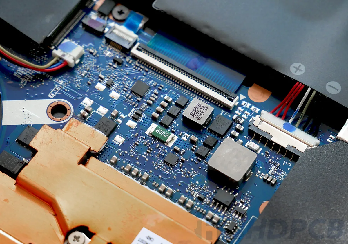
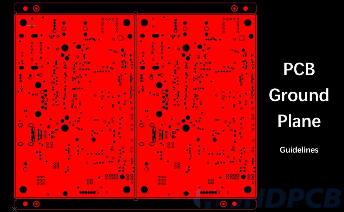
A common technique is to use a ground plane on pcb, which is a large piece of copper on a printed circuit board. PCB manufacturers usually cover all surfaces that have no component or trace with the copper ground plane. For example, if your PCB is made up of two layers, the ground plane on both sides of pcb should be placed on the bottom layer of the PCB, according to standard PCB rules, while components and signal traces are on the top layer.

PCB areas with&without common ground

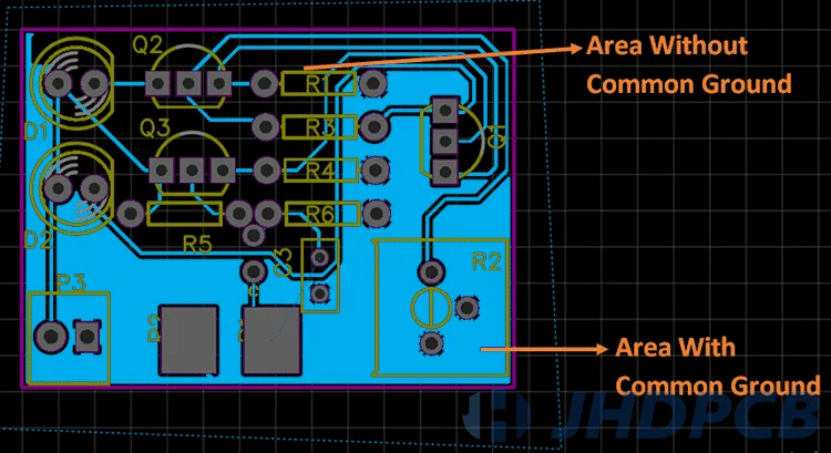
A ring of conductive material formed by the ground plane is best avoided, as it makes the ground plane more sensitive to electromagnetic interference (EMI). This conductive ring acts as an inductor, and an external magnetic field can cause an electric current known as a ground loop. A conductive ring can occur if you place the ground plane over the entire bottom layer and then remove the parts containing electronic components. To avoid this problem, keep the traces as short as possible and arrange the ground plane so that it passes completely under the traces, as shown in the traces illustration. It may be necessary to adjust the layout of tracks and components to avoid creating conductive rings.
The ground plane can also be located on both sides of the PCB, with the ground plane on the component side connected to the supply voltage, while the ground plane on the other side remains connected to ground. The ground plane is connected to the ground pins of components and connectors to maintain the ground voltage at the same level across the entire PCB.
On two-layer PCBs, you can use more than one copper ground plane, but they must all be connected to the power supply independently. This avoids ground loops and keeps the layers separate.

When there are ground planes on both sides of the PCB, they are connected by vias at different points on the board. These vias are holes that pass through the PCB and connect the two sides to each other. They allow access to the ground plane from any location compatible with a through-hole.

Via Holes under an IC Body

The use of vias can help avoid ground loops. They connect components directly to ground points, which are connected with low impedance to all other ground points in the circuit. They also reduce the length of return loops.
Copper pieces, such as ground planes, can resonate at a quarter of the wavelength of the frequency of the current flowing through them. Placing tapping vias around the ground plane at specific intervals can help control this phenomenon. A good rule of thumb is to place the grounding vias at one-eighth of the wavelength or less. This is because a stub on a trace only begins to cause problems at one-eighth of a wavelength.
In case the circuit board does not have vias, a small drill can be used to drill several holes. A copper wire is then passed through the holes and soldered to create a connection on both sides.

All connectors on the printed circuit board must be grounded. In the connectors, all signal conductors must run in parallel. For this reason, it is necessary to separate the connectors using ground pins. Each board will probably need more than one ground pin for the connector. The presence of only one pin can cause impedance mismatch problems, resulting in oscillations.

Current bounces can affect system performance and increase the contact resistance of the connector pin over time. The contact resistance of each pin of a connector is low but can increase over time.  For this reason, it is ideal to use multiple ground pins. About 30-40% of the pins in a PCB connector should be ground pins.

Connectors come in different pitches and can have different numbers of pin rows. The pins of a connector can also be parallel to the PCB surface or at right angles to it.

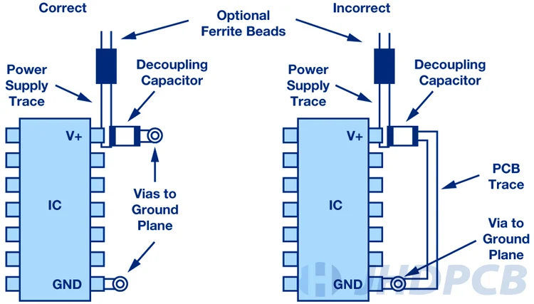
Printed circuit boards contain one or more integrated circuits that require power to operate. These chips have power pins that connect them to an external power source. They also have ground pins to connect them to the ground plane of the printed circuit board. Between the power and ground pins is a decoupling capacitor, which is used to dampen fluctuations in the voltage supplied to the chip. The opposite end of the decoupling capacitor is connected to the ground plane.

One of the main reasons for using decoupling capacitors is related to functionality. A decoupling capacitor can act as a charge storage device. If the integrated circuit (IC) needs additional current, the decoupling capacitor can supply it through a low inductance path. For this reason, it is recommended that decoupling capacitor components be placed near the IC’s power supply pins.
Another major reason for using decoupling capacitors is to minimize noise caused by ground plane pairs and the power supply, and to reduce EMI. There are two main issues that can lead to this noise:
A decoupling capacitor that does not provide sufficient current, resulting in a transient voltage drop across the IC’s power supply pin.
Intentionally shared current between the ground planes and the power supply via a fast switching signal.

Placement of decoupling

However, to get the best out of decoupling capacitors, their location needs to be carefully considered: they should be distributed across the PCB, with some located close to IC ground or close to IC ground. In addition, the decoupling capacitors used should have the highest capacitance values and all be of the same value. For maximum performance and functionality, a high equivalent series resistance (ESR) should be combined with normal capacitors.

When can I avoid using a PCB ground plane?

As mentioned earlier, it is possible to design a PCB without a ground plane. If you are developing a proof of concept or prototype and the design just needs to work well, you can do without a ground plane on the PCB as long as the design works with development boards and a breadboard configuration. If you want to develop a product for commercial use, you may run into problems with excessive noise or radiation emissions without a ground plane on the PCB.
In some cases, it is much easier to solve the problem by using a ground plane instead of a power plane. This is an important distinction and one of the reasons I try not to make “always/never” statements in this area: The design may work as intended, but that doesn’t mean it’s quiet or marketable.
That being said, there are some cases where you can probably do without a ground plane on the PCB and the design will work well and have low emissions:

  • The PCB passes the EMC tests.
    The design passes the EMC tests if it is populated with modules, wires/cables, and development boards. If the noise of the design is low enough to pass the EMC tests under these conditions, it will be very difficult to degrade it once it is integrated on a two-layer PCB.
  • DC only.
    DC designs can usually do without a ground plane on the PCB, provided the system does not use high-power or switching regulators. These designs can be sensitive to electromagnetic interference, but it can be filtered out so that it is not noticeable. In addition, the design does not have to deal with the signal integrity and power supply issues associated with digital cards.
  • Low density, tight coupling.
    If the board density is low enough, it is likely that a ground wire can be routed adjacent to the signals/power supplies, and a ground plane on the board is not required. If the design density is low enough and the signal speed is low enough, it is possible to pass the EMC tests.
  • All signals are differential.
    Differential signals do not need to be grounded because of the impedance and low noise in differential mode, but grounding is useful. A digital interface converter module or isolator module are examples of designs.

How to fix wrong PCB ground plane?

There are cases where copper castings are used in sections instead of separate planes, which can make it difficult to achieve design goals (well-defined impedance; return paths; EMI shielding and attenuation; decoupling and stable power supply). Problems with routing and maintaining a well-defined ground plane can cause high loop inductance, leading to EMI interference. The following table shows the solution to PCB ground plane problems.

FeatureProblemSolution
Routing over splits in ground planesCreates a long return path with high loop inductance → strong EMI and crosstalk.Minimize splices and trace returns on the board to ensure a uniform ground plane.
Copper pour regions without uniform planeThe return path is difficult to trace and results in poorly defined impedance.Join castings, fill gaps with copper castings, and trace only homogeneous areas
Small overlap between power rails and groundOn high-speed boards, this results in poor decoupling due to low capacitance between levels.Ensure that the power and ground planes overlap and are distributed throughout the PCB.
Inadequate Ground Plane CoverageThe ground plane does not cover a significant area of the PCB, resulting in insufficient grounding and potential noise issues. Increase the coverage of the ground plane by adding additional copper fills or enlarging the existing ground plane. Ensure that the ground plane connects to all ground points and components that require grounding.
Ground Plane DiscontinuityThe ground plane has gaps, voids, or breaks, which can disrupt current flow and introduce noise into the circuit.Fill the gaps or voids in the ground plane by adding copper traces or conducting vias to ensure a continuous path for current flow. Verify that there are no unintended breaks or cuts in the ground plane.
Inadequate Ground Plane PlacementThe ground plane is located far from critical components or high-current traces, leading to longer return paths and potential EMI issues.Ensure that the ground plane is placed close to critical components and high-current traces to minimize the loop area and reduce the path for noise induction. Consider adjusting the component placement or rerouting traces if necessary.

Adding a ground plane to a printed circuit board is a simple, inexpensive, and highly effective way to design electronic devices with increased signal integrity, accuracy, and resistance to interference. If you are not already using a ground plane, please consider the above information and advice when designing your next printed circuit board.
Hopefully you have now cleared up all your doubts and questions about PCB grounding plans. Do your research and choose the best option for your PCB. Remember not to design the wrong PCB layout in a hurry. Take your time and prioritize your needs. Choosing JHD is also a wise decision because we have the following advantages:

  • PCB Design Review-
    We can review your PCB design to ensure proper placement, coverage, and integrity of the ground plane. Our experts will examine the layout for any potential issues and suggest improvements to optimize signal integrity.
  • Ground Plane Optimization-
    We can help you optimize the ground plane design by adjusting its size, thickness, and placement according to your specific requirements. This includes ensuring proper grounding for critical components, minimizing loop areas, and reducing the risk of interference.
  • Design Guidelines and Standards-
    We stay updated with the latest design guidelines and industry standards, allowing us to provide you with recommendations aligned with best practices. Our expertise enables us to address any potential concerns related to the ground plane effectively.

By collaborating with JHD, you can benefit from our extensive experience in PCB design and manufacturing. We understand the importance of a well-designed ground plane and can provide you with the guidance and support you need to achieve optimal results. Don’t hesitate to reach out to us for assistance in incorporating a ground plane into your next PCB project.

Get a PCB Quote Now

Open high-quality PCB manufacturing services in JHDPCB

Leave a Comment