CARBON INK

Key Points Of Carbon Ink PCB

directory

What is Carbon Ink PCB?

What is Carbon Ink PCB

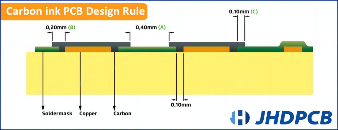
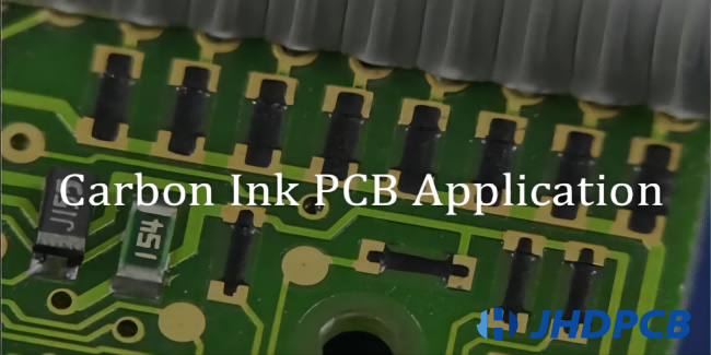
Carbon Ink PCB, also known as carbon conductive PCB, is circuit board that utilize carbon ink as a replacement for traditional solder plating methods such as Electroless Nickel Immersion Gold (ENIG) or Hot Air Solder Leveling – Lead Free (HASL). The purpose of carbon ink on pcb is to provide conductivity between copper pads, serving as a conductor to connect traces on the board. It can function as a resistor between traces or between traces and components.

The production of Carbon Ink PCBs involves several key factors such as printing, baking, and resistance control. The carbon ink is applied onto the copper pads of the PCB substrate and then cured to form a conductive pattern with a carbon film. This process helps create reliable connectivity and functionality.

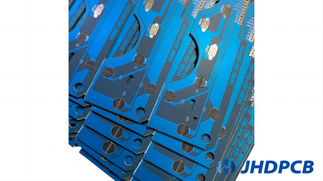
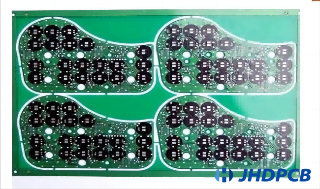
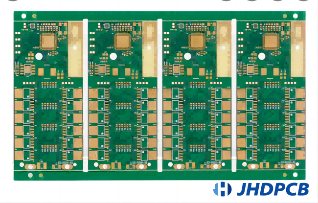
Carbon Ink PCBs can be applied to various types of PCB substrates, including flexible circuits, rigid-flex boards, and rigid PCBs made of materials like polyimide, polyester, FR-4, FR-5, and PTFE laminates. The use of carbon ink allows for fine resolutions, with trace widths and spacing as small as 100μm.

These PCBs find applications in different areas such as keyboard contacts, LCD contacts, and jumpers. The carbon contacts on Carbon Ink PCBs are typically round in shape, with diameters ranging from 2mm to 8mm. It is crucial to maintain carbon widths at 75% of the nominal value for optimal performance.

In terms of cost-effectiveness, Carbon Ink PCBs provide a viable solution compared to more expensive plating methods like gold. Due to the reduced production expenses linked with PCB fabrication, they have gained popularity as a preferred option in the market. Through rigorous inspections, tests, aging tests, and other technical processes, Carbon Ink PCBs can offer long-lasting and reliable performance.

Overall, Carbon Ink PCBs offer an alternative approach to achieve conductivity and connectivity in circuit boards, making them suitable for various electronic applications.

What are the characteristics of Carbon Ink PCB?

  1. Simple production process:
    Carbon Ink PCB adopts a screen printing process, which is relatively simple compared to other PCB manufacturing methods. The process includes applying one or two layers of conductive carbon ink designs onto a single-layer printed circuit board.
  2. High-density wiring:
    The addition of conductive carbon ink patterns enables high-density wiring on the PCB. This allows for the realization of complex circuitry and integration of various components in a compact space.
  3. Multifunctional applications:
    The conductive patterns printed on Carbon Ink PCBs can fulfill various functions like resistors, key switch contacts, and electromagnetic shielding layers. This adaptability makes it ideal for a range of electronic devices that need to be compact, lightweight, and multifunctional.
  4. Wide range of applications:
    Conductive pcb carbon ink finds applications in various electronic devices and components such as silica gel keys, potentiometer sliders, remote controllers, electronic organ tuning film, PCB keys, touch screens, inductive pens, and conductive circuit boards.
  5. Simplified production process:
    Carbon Ink PCB eliminates the need for interconnection holes found in traditional plated through-hole (PTH) PCBs. This simplifies the production process and allows direct steel mesh printing. It also enables the use of lighter materials such as phenolic cardboard.
  6. Shortened production cycle and reduced costs:
    Carbon Ink PCB can significantly shorten the production cycle of double-sided PCBs. It also reduces the overall volume of the device, increases assembly efficiency, and lowers production costs. Additionally, it is suitable for high-volume PCB assembly production, thus improving productivity.
  7. Environmental friendliness:
    Carbon Ink PCB production does not generate the three wastes (waste water, waste gas, and solid waste). This contributes to environmental friendliness and aids in the reduction of pollution.

It is worth noting that the technical specifications and testing methods for Carbon Ink PCB are discussed in standards such as IEC1249-5-4, SJ/T11171-98 issued by China’s electric industry, and technical specifications provided by companies like Hitachi, Toshiba, Panasonic, and ink manufacturers such as Coates, Acheson, Asahi.

Carbon Ink PCB vs Hard Gold PCB

Carbon Ink PCB vs Hard Gold PCB

When comparing Carbon Ink PCBs to Hard Gold PCBs, there are several key differences to consider: 

Carbon Ink PCB: Carbon Ink is used as a conductor on the copper pads, offering a low-cost alternative to traditional surface finishes like Hard Gold. The carbon ink is applied through a screen printing process, which is relatively simple and cost-effective.

Hard Gold PCB: Hard Gold is a high-quality surface finish that provides excellent conductivity and corrosion resistance. Nevertheless, it is a costly choice because of the intricate electrolytic plating process it entails.

Carbon Ink PCB: Carbon Ink PCBs exhibit high robustness and durability. The dry carbon conductive ink used in these PCBs can withstand over 1 million keyboard push button operations or more than 100 edge connector insertions without showing signs of wear or increased resistance.

Hard Gold PCB: Hard Gold is renowned for its superb conductivity and resistance to corrosion. Nonetheless, it might not provide the equivalent degree of mechanical robustness as Carbon Ink PCBs, particularly concerning repetitive operations and wear.

Carbon Ink PCB: The plating process for Carbon Ink PCBs involves a simple screen printing process to apply the carbon ink onto the copper pads. This process is relatively easy and cost-efficient compared to the complex electrolytic bath required for Hard Gold plating.

Hard Gold PCB: Hard Gold plating requires a more intricate and time-consuming electrolytic plating process. This process involves multiple steps, including cleaning, activation, and gold deposition, making it more complex and costly.

Carbon Ink PCB: One challenge with Carbon Ink PCBs is ensuring that the cured and dry carbon conductive ink maintains adhesion and conductivity during subsequent assembly processes. Special care and different cleaning steps may be required to prevent any loss of adhesion or conductivity during soldering or solvent cleaning.

Hard Gold PCB: Hard Gold provides excellent adhesion and conductivity, ensuring reliable performance during assembly and subsequent processes. It provides a steady and resilient surface coating that is less prone to deterioration.

Carbon Ink PCB: Carbon ink for pcb is generally considered more environmentally friendly compared to the processes involved in hard gold plating, which often require the use of harsh chemicals and extensive rinsing processes. The simpler application process of carbon ink may result in reduced environmental impact.

Hard Gold PCB: The electrolytic plating process used for hard gold PCBs can involve the use of various chemicals and materials, which may have a greater environmental impact compared to the application of carbon ink.

Carbon Ink PCB: When considering applications in warmer climates, the viscosity stability of the carbon ink circuit surface becomes an important factor. Carbon ink PCBs must maintain good viscosity stability to ensure consistent performance in varying temperature conditions.

Hard Gold PCB: Hard gold surface finishes are known for their resistance to corrosion and oxidation, making them suitable for a wide range of environmental conditions, including high-temperature applications.

Carbon Ink PCB: Carbon ink PCBs are well-suited for applications where cost efficiency and mechanical durability are key considerations, such as consumer electronics, membrane switches, and other applications where repeated button operations are common.

Hard Gold PCB: Hard gold PCBs are often chosen for high-reliability applications where excellent conductivity, corrosion resistance, and stable performance over time are critical, such as aerospace, medical devices, and industrial equipment.

Carbon Ink PCB: The screen printing process used for applying carbon ink offers greater flexibility and simplicity in the manufacturing process, making it easier to implement design changes and iterate quickly during prototyping.

Hard Gold PCB: The complex nature of hard gold plating may limit the flexibility and ease of making design changes during the manufacturing process, potentially leading to longer lead times and higher costs for design modifications.

In summary, the comparison between Carbon Ink PCBs and Hard Gold PCBs reveals distinct differences in cost, robustness, manufacturing processes, environmental impact, application specificity, and manufacturing flexibility. Carbon Ink PCBs offer a low-cost, durable, and environmentally friendly option, suitable for applications with repeated operations. Meanwhile, Hard Gold PCBs provide excellent conductivity, corrosion resistance, and stability, making them ideal for high-reliability applications. The decision between the two options relies on particular application requirements, taking into account aspects like expenses, longevity, conductivity, and ecological footprint. 

The Advantages and disadvantge Of Carbon Ink PCB

Carbon ink PCBs have both advantages and disadvantages. Here are some of them:

Advantages:
  • Cost-effective: Carbon ink PCBs are generally more cost-effective compared to traditional copper-clad PCBs.

    The materials used in carbon ink PCB production, such as carbon-based conductive ink, are often less expensive than copper. This could lead to substantial cost reductions, particularly for mass production scenarios.

  • Flexibility and Design Freedom: Carbon ink PCBs offer greater flexibility and design freedom compared to rigid copper-clad PCBs. They can be easily manufactured on flexible substrates, allowing for curved or irregular shapes. This makes them ideal for applications that require bendable or conformal electronics, such as wearable devices, flexible displays, and medical sensors.

  • Lightweight: Carbon ink PCBs are lightweight due to the reduced amount of material used in their construction. This property is particularly advantageous in weight-sensitive applications such as aerospace, automotive, and portable electronics, where reducing overall weight is crucial for performance and efficiency.

  • Good for Low-frequency Applications: Carbon ink PCBs have lower conductivity compared to copper. However, this can be an advantage in certain low-frequency applications where high conductivity is not necessary. For example, they are well-suited for low-frequency RFID antennas, touch sensors, and other similar applications.

Disadvantages:
  • Limited Conductivity: Carbon ink has inherently lower conductivity compared to copper. This can result in higher resistance and voltage drop along the conductive traces, which may limit its use in high-frequency applications or applications that require low resistance paths. Copper-clad PCBs are generally preferred for high-frequency electronic circuits or applications with strict impedance requirements.

  • Limited Power Handling Capacity: Due to their lower conductivity, carbon ink PCBs may not be suitable for high-power applications. They may struggle to handle high currents without experiencing significant power losses or excessive heating. Copper-based PCBs, with their superior conductivity, are better suited for high-power applications where efficient power transmission is critical.

  • Durability Concerns: Carbon ink can be more prone to wear off over time, especially under conditions of mechanical stress or repeated usage.

     In applications where there is friction or rubbing against the conductive traces, such as sliding contacts or switches, the carbon ink may degrade or lose conductivity over the long term. This can lead to potential reliability issues and may require periodic maintenance or replacement.

  • Limited Availability and Customization Options: Carbon ink PCBs may have limited availability compared to traditional copper-clad PCBs. The production processes and supply chains for carbon ink PCBs are not as widespread or mature. As a result, they may have longer lead times and limited options for customization compared to copper-clad PCBs, which are widely available and can be easily tailored to specific design requirements.

In summary, carbon ink PCBs offer advantages in terms of cost-effectiveness, flexibility, lightweight design, and suitability for low-frequency applications. Nevertheless, they also come with constraints regarding conductivity, power capacity, robustness, and accessibility. Careful consideration of these factors is necessary when deciding whether to use carbon ink PCBs or traditional copper-clad PCBs for a particular application.

What's the application of Carbon Ink PCB?

application of Carbon Ink PCB

Carbon Ink PCBs are widely used in various applications due to their versatility and effectiveness. Here are some detailed applications of Carbon Ink PCBs:

  1. RF Shielding: Carbon Ink PCBs are utilized for their conductivity and shielding properties in applications where radio frequency interference needs to be minimized or controlled.
  2. Keypads and Keyboards: Carbon Ink is often used to create the conductive traces on keypads and keyboards, providing reliable contact points for user input.
  3. Remote Controllers: In devices like TV remote controllers, garage door controllers, and other remote devices, Carbon Ink PCBs are used to create tactile switches that provide feedback to the user when pressed.
  4. Automotive Vehicles: Carbon Ink PCBs find applications in automotive electronics for functions such as sensor control, interface panels, and other electronic components in vehicles.
  5. Industrial Engine Control: Carbon Ink PCBs are used in industrial settings for engine control systems, providing reliable connections and signal transmission for critical operations.
  6. Welding Equipment: Carbon Ink PCBs are employed in welding equipment for control panels, interface circuits, and other electronic controls required in welding processes.
  7. Consumer Electronics: They are utilized in various consumer electronic devices for creating touch-sensitive interfaces, control panels, and input devices due to their reliability and cost-effectiveness.
  8. Medical Devices: Carbon Ink PCBs are employed in medical equipment and devices for control interfaces, input systems, and other electronic components due to their durability and stable electrical properties.
  9. Household Appliances: They are integrated into household appliances such as microwave ovens, washing machines, and air conditioners for control panels and user interfaces.
  10. Security Systems: Carbon Ink PCBs play a role in security systems and access control devices, providing reliable connections and switch mechanisms for keypads and control panels.
  11. Industrial Controls: They are used in various industrial control systems for machinery, equipment, and process control, ensuring reliable electrical connections and signal transmission.
  12. Aerospace Applications: Carbon Ink PCBs find use in aerospace applications for instruments, control panels, and interface circuits due to their ability to withstand harsh environmental conditions.

To conclude, the adaptability and dependability of Carbon Ink PCBs render them appropriate for diverse applications spanning various industries.

Carbon Ink Printed Circuit Board Design Guidelines

  1. Design Carbon to Carbon Spacing:
    This rule specifies that a minimal isolation or spacing of 0.8mm (16 mil) must be maintained between the copper elements of typical carbon finger contacts. Advanced carbon PCB manufacturing capabilities allow for smaller minimum values, such as reaching an advanced minimum carbon to carbon spacing of 0.3mm (12 mil), albeit with a longer lead time.
  2. Min Carbon Line Width:
    This rule sets the minimum width of carbon lines at 0.3mm (12 mil). It indicates that any carbon line in the design should not have a width less than this specified value.
  3. Min Carbon on Copper Overlap:
    The guideline requires a minimum overlap of 0.2mm (9 mil) between carbon and copper elements. This means that carbon elements should overlap with copper by at least 0.2mm.
  4. Min Carbon on Solder Mask Overlap:
    This rule specifies a minimum overlap of 0.1mm (4 mil) between carbon elements and the solder mask layer. It states that there should be an overlap of at least 0.1mm between carbon and the solder mask layer.

These design rules are crucial for ensuring the proper functioning and reliability of carbon ink printed circuit boards. Designers should adhere to these guidelines when working on the design of carbon ink printed circuit boards to ensure that the boards meet the desired performance standards.

Design Rule Alphabet Value
Design Carbon to Carbon Spacing A 0.4mm (16 mil)
Min Carbon Line Width 0.3mm (12 mil)
Min Carbon on Copper Overlap B 0.2mm (9 mil)
Min Carbon on Solder Mask Overlap C 0.1mm (4 mil)

Key points of carbon ink printing process

Key points of carbon ink printing process


  • Operators must wear gloves made of suitable materials to prevent contamination of the printed PCBs and ensure personal safety.
  • The work area should be kept clean, and operators need to ensure that the equipment surfaces are free from dust, garbage, and other debris to maintain high printing quality standards.
  • Screen-printing speed, back-to-ink speed, and suction pressure should be precisely controlled within the best range to achieve optimal printing effects. These parameters should be carefully adjusted and tested to ensure the desired print quality.
  • Screen stencils, scrapers, and carbon ink must meet specific requirements as per the instructions provided by the MI engineer or the manufacturer’s guidelines to ensure precise and consistent results.
  • Before use, it is essential to completely blend the carbon ink to guarantee consistent uniformity. The viscosity of the ink must be checked using a viscometer to ensure it falls within the required range. Following usage, it is advisable to promptly seal the ink to preserve its quality for subsequent use.
  • Prior to printing, all PCB boards must undergo a thorough cleaning process to remove plate grease, oxide, and other pollutants that may affect the adhesion and quality of the printed carbon ink traces. Additionally, QA confirmation is required for all carbon plates before official production.
  • The specified drying temperature and duration for carbon PCBs is 150°C for 45 minutes, ensuring thorough curing and bond strength. Similarly, carbon ink holes require drying at 150°C for 20 minutes to achieve the desired properties.
  • After the release from the oven, the operator should inform the QA team to check the carbon resistance and perform adhesion tests to verify the quality of the printed traces. This step ensures that the conductive traces meet the required quality standards for electrical performance and durability.
  • Each carbon ink screen version is limited to a maximum of 2,500 printing times. Upon reaching this limit, the screen must be returned to the network room for re-drying or replacement, maintaining the integrity of the printing process and the quality of the printed PCBs.

FAQ of Carbon Ink PCB

Carbon ink plays a crucial role in PCB manufacturing by being used to create carbon conductive ink PCBs. This particular ink creates conductive paths on the board, enabling the transmission of electrical signals.

Carbon ink is applied to PCBs through a printing process, resulting in the creation of carbon ink layers on the board. These layers provide conductivity and offer advantages such as cost-effectiveness and adaptability to different substrate materials.

Yes, there are reputable carbon ink pcb manufacturers in China specializing in producing China carbon ink PCBs. These manufacturers handle requests for China carbon ink PCB quotes by evaluating the specific design requirements provided by the client. They offer tailored solutions and high-quality production to meet the client’s needs. For example, our company, JHDPCB, is well-known for providing custom China carbon ink PCBs and can offer detailed quotes and technical support based on your requirements.

Carbon ink can indeed be used for repairing PCBs, including in China. When considering carbon ink PCB repair, factors such as the extent of damage, application technique, and compatibility with existing circuitry need to be carefully evaluated to ensure effective restoration of the PCB’s functionality.

Carbon Printing is a photographic printing process used to create black and white prints with exceptional tonal range, primarily in fine art photography. On the other hand, Carbon Ink PCB is a type of circuit board that utilizes carbon ink as a replacement for traditional solder plating methods, providing conductivity and acting as a conductor or resistor in electronic devices.

To summarize, Carbon Ink PCBs provide a flexible and economically viable solution for a wide range of electronic applications. With their unique characteristics of flexibility, affordability, and ease of prototyping, Carbon Ink PCBs provide a practical alternative to traditional copper-based PCBs. Their applications in devices such as keypads, sensors, and membrane switches showcase the adaptability and utility of Carbon Ink PCBs in modern electronics. Understanding the benefits and considerations of Carbon Ink PCBs is essential for designers and manufacturers looking to optimize their circuitry solutions with this innovative technology.

At JHDPCB, we take pride in our expertise and capabilities in Carbon Ink printing PCB manufacturing. Our company is equipped with state-of-the-art facilities and a highly skilled team that ensures top-notch quality and precision in every product we deliver. Our commitment is to deliver outstanding customer service and customized solutions that align with the individual requirements of our clients.Whether you are in need of custom Carbon Ink PCBs or require technical consultation, we welcome you to reach out to us for any inquiries.

Get a PCB Quote Now

Open high-quality PCB manufacturing services in JHDPCB

Leave a Comment