Importance of PCB aspect ratio in PCB manufacturing
Before delving into aspect ratios, let’s take a moment to revisit the significance of PCB via aspect ratio and annular rings in your design.
Vias serve as holes drilled through the traces of different layers in a Printed Circuit Board, enabling connections between these layers. They are particularly prevalent in HDI multi-layered PCBs, where interlayer connectivity is crucial. Vias come in various forms, including blind, buried, and through-hole vias.
Blind vias establish connections between an outer layer and an internal layer of the PCB, without extending further. In a four-layered PCB, the first two layers will have drilled holes through the traces, while the third and fourth layers will not.
Buried vias, on the other hand, connect two or more internal layers exclusively. In our four-layered PCB example, the second and third layers would be connected via drilled holes, whereas the outer layers (first and fourth) would lack any visible holes.
Through-hole vias, as the name suggests, are drilled through the entire board, connecting the outermost layers together or establishing various combinations of connections between the four layers.
Once the vias are appropriately designed into the PCB, the next step involves drilling at each via location. This is where annular rings come into play. An annular ring refers to the copper ring encircling the drilled hole of the via, providing a surface for component mounting or enabling plating. The size of the annular ring directly impacts the connection surface. It is a seemingly simple yet critical aspect of the manufacturing process.
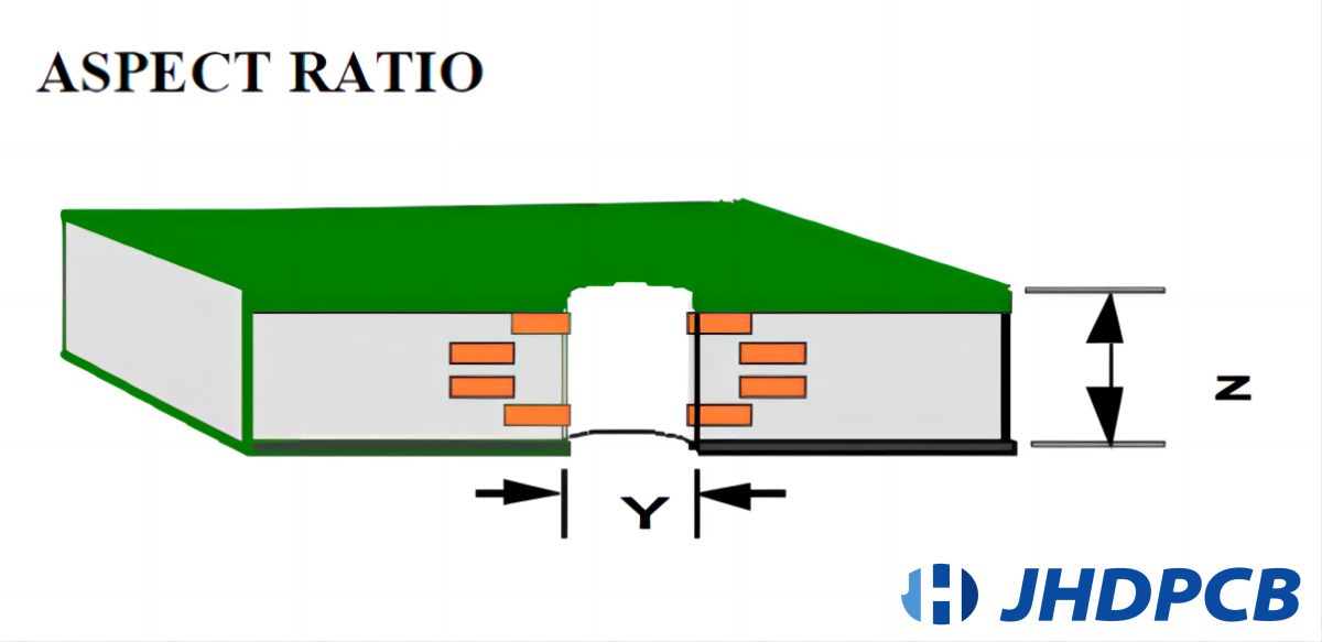
Now let’s turn our attention to aspect ratio of pcb, which represent the Ratio of drilling depth to drilling diameter. This ratio holds significance due to its effect on plating within the vias, as well as its interaction with the annular rings.
Consider a board with a thickness of 0.2″ and a via drill diameter of 0.02″. In this case, the aspect ratio pcb would be 10:1. As the aspect ratio increases, more plating surrounds the via compared to the interior drilled portion. Consequently, the risk of cracking due to z-axis expansion during soldering increases. Maintaining a lower aspect ratio ensures consistent plating throughout the via and enhances the overall strength and durability of the Printed Circuit Board.
What is the aspect ratio in pcb?
The aspect ratio (AR) is the ratio of the drilling depth to the diameter of the smallest hole drilled in the same PCB. Drilling methods can be CNC mechanical drilling or laser drilling. The drilling depth does not take into account copper metallization, solder mask, surface finish or silk screen. In PCB manufacturing, the higher the ratio, the more difficult it is to achieve reliable metallization.
Some people may think that the PCB Aspect Ratio definition is the ratio of board thickness and hole diameter, but this only applies to the through-hole aspect ratio. If it is buried and blind holes have nothing to do with the overall thickness of the board, so to be precise, PCB Aspect Ratio is the ratio of the depth of the hole to the diameter of the hole.
The aspect ratio pcb design is an important consideration in its design and manufacturing. It affects various aspects of the PCB, including its form factor, layout, and manufacturability.
The aspect ratio is particularly relevant when dealing with PCBs that have high-density components or complex designs. It impacts factors such as signal integrity, thermal management, and the ability to route traces effectively. High aspect ratios may require additional considerations during fabrication, such as specialized drilling techniques for vias or increased attention to ensure proper solder flow during assembly.
Different applications and design constraints may dictate specific aspect ratio requirements. It is crucial to consider the PCB manufacturer’s capabilities and guidelines when determining the appropriate aspect ratio for a given design.
Importance of PCB Aspect Ratio.
The aspect ratio of a PCB is of significant importance due to its impact on the plating process. Plated holes, including through-holes and blind/buried vias, serve as essential elements in the PCB layout, acting as connection points between different layers. However, during the actual plating process, certain challenges arise when dealing with thicker PCBs and smaller holes.
The aspect ratio of the PCB plays a crucial role in determining the difficulty of plating. Thicker PCBs make it more challenging for the plating solution to flow uniformly through the small holes. This can result in uneven plating, particularly in the center areas of the holes, which are known as the low current areas. These areas receive less plating and may lead to weak connections or unreliable performance of the PCB.
The aspect ratio directly affects the plating process. It is defined as the pcb drill aspect ratio hole depth to drill hole diameter. Achieving uniform plating throughout the holes becomes increasingly challenging with higher aspect ratios.
To overcome these challenges, advanced equipment, more expensive additives, and improved manufacturing processes are often required. PCB suppliers with the capability to handle higher aspect ratios demonstrate their expertise and reliability in producing PCBs with reliable and consistent plating. They invest in specialized equipment and employ advanced techniques to ensure that the plating process is successfully carried out, even with higher aspect ratios.
In summary, the aspect ratio of a PCB is crucial because it affects the plating process. Higher aspect ratios pose challenges in achieving uniform plating, necessitating advanced equipment and techniques. Therefore, when evaluating the capabilities of a PCB supplier, considering the aspect ratio is indispensable to ensure reliable and high-quality PCB manufacturing.
How to calculate aspect ratio in pcb?
To determine the aspect ratio, you must determine in advance the width and length of the image or video. Once you have determined these two measurements, enter them into the pcb aspect ratio calculator above to determine the aspect ratio. All calculations are done automatically to ensure efficiency, accuracy and smoothness!
Portrait vs Landscape:
The aspect ratio calculator can also determine the mode of the image or video. Calculations are based on parameters. The mode for images and videos with a height greater than width is “landscape,” while the mode for images and videos with a width greater than height is “portrait.”
Routing.
The best strategy in prototyping is to lay traces over short distances, taking into account the complexity of the PCB. It has been possible to use mentally difficult buried vias and to place vias in high-voltage pads. However, invisible and buried vias are more difficult to produce because they require an additional drilling process and the drilling process can leave deposits in the hole, leading to production problems. Normal vias are usually too large to be integrated into the small mounting surfaces of high-current systems. Pcb microvia aspect ratio can therefore cause all these problems:
- The manufacture of microvias is simpler than that of small illusion and immersion wafers.
- Microvias work with small surface-mountable pads, which is particularly useful for circuits with a large number of pins, such as Pin-Grid-Array (BGA) circuits.
- Because of their size, microvias can also help reduce electromagnetic interference and other circuit design problems.
Microvias are a complex PCB manufacturing process, and if your circuit board doesn’t need them, it’s best to stick with traditional vias to save money. However, if your circuit is very thick and you need extra space, you should consider whether or not microvias might be useful. As always, before building a PCB with microvias, check their specifications with your contractor.
Calculator Screen Size:
Is your 17:8 HDTV widescreen display attempting to find out the enhanced knowledge? This program calculates 3 out of 4 centimeters and inches for you. Just input any existing screen size and compute the others.
1.choice of aspect ratio Aspect
Aspect ratio
Selection of hyperparameters
High-definition 4K (3840 to 2160)
Full HD (1920 to 11080)
HD Ready (1280 vs 720)
WUXGA (1920 vs. 11200)
UWQHD (3440 vs. 1440) UWQHD
Anamorphic
NTSC/PAL
2.Calculate
Select a known measurement (hexagonal pattern, height or width) and calculate the other two.
Diagonal.
Cm / cm = calculate
Length
Cm / cm = calculate
Diameter
cm / cm = calculate
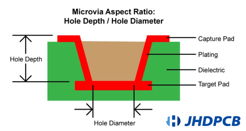
What is Microwell Aspect Ratio?
The pcb via hole aspect ratio is the ratio of the depth of the hole to its diameter (the depth of the hole to its diameter). For example, the aspect ratio of a standard 0.071″ thick PCB with a 0.023″ hole would be 3:1. This ratio is used as a guideline to ensure that the manufacturer does not exceed the capacity of his equipment when drilling holes. For standard holes, the aspect ratio should normally not exceed 10:1, so that a 0.062″ hole can be drilled in a 0.006″ diameter PCB.
When using a microvias, the aspect ratio is significantly different due to size and depth. Masking small holes can be difficult, and attempting to mask a small hole through 10 layers of PCB can cause many problems for the PCB manufacturer. However, if the hole goes through only two of these layers, metallization becomes much easier. The IPC used to define a micro-hole by its size, which is 0.006 inch (0.15 mm) or less. However, over time this size became common, and the IPC decided to change the definition to avoid having to constantly update the specification as technology evolved. Now the IPC defines a microvias as a hole with an aspect ratio of 1:1, provided the depth of the hole does not exceed 0.00% or 0.25mm.
How a Microvia Can Help with the Trace Routing on Your Circuit Board?
The general rule in PCB design is to put more vias in a smaller area as PCB technology becomes denser. This has led to the use of blind and buried vias and the incorporation of vias into surface mount pads. However, blind and buried through-holes are more difficult to fabricate due to the additional drilling steps, and drilling can leave material in the holes, leading to production defects. In addition, the usual interlayer holes are usually too large to fit into the small mounting inserts of today’s high-density devices. However, with micro-wires, all these problems can be solved:Microvias are easier to manufacture thaen small blind and buried vias.
- Microvias fit onto small surface-mount boards and are therefore particularly useful for components with a large number of pins, such as ball grid arrays (BGAs).
- Because of their small size, more traces can be routed around the microvias.
- Because of their size, microvias also help to reduce electromagnetic interference and improve other aspects of signal integrity.
Microvias are an advanced method of manufacturing printed circuits. If your board does not require micro pins, you will of course use standard pins to keep costs low. However, if your design is very dense and you need extra space, you should consider whether using micro conductors could be beneficial. As always, it is advisable to check the options with your contract manufacturer before designing a printed circuit board with micro projectors.
What factors affect PCB Aspect Ratio?
The aspect ratio of a PCB (Printed Circuit Board) is influenced by several important factors, which collectively determine the ratio of its length to its width. These factors directly impact the design and manufacturing considerations associated with the PCB. Let’s delve into each factor in more detail:
PCB Thickness:
The thickness of the PCB material is a crucial factor in determining the aspect ratio. Thicker PCBs have a lower aspect ratio, as the increased thickness limits the available space for routing traces and placing components. Conversely, thinner PCBs provide more flexibility in achieving higher aspect ratios.
Hole Diameter (Via Diameter):
The diameter of the holes or vias used in the PCB also affects the aspect ratio. Smaller hole diameters allow for higher aspect ratios, as they require less space vertically. However, there are practical limitations to the smallest hole sizes that can be reliably drilled, which must be considered in the design.
Board Area:
The overall size or area of the PCB plays a role in determining the aspect ratio. Larger boards tend to have more flexibility in achieving higher aspect ratios since there is more available space for routing traces and accommodating components. Conversely, smaller boards may face space constraints, limiting the achievable aspect ratio.
PCB Manufacturer's Manufacturing Capabilities:
The manufacturing capabilities of the PCB manufacturer influence the achievable aspect ratio. Different manufacturers may have varying abilities to handle specific aspect ratios based on their equipment, technologies, and expertise. Consulting with the manufacturer is very important, which can understand their capabilities and any limitations they may have.
PCB Design Guidelines and Standards:
Various industry-specific design guidelines and standards provide recommendations and constraints for PCB aspect ratios. These guidelines are established based on best practices and ensure reliable fabrication and assembly processes. Adhering to these guidelines helps maintain design integrity and manufacturability.
Trace Width and Spacing:
Although not directly related to aspect ratio, the width and spacing of the traces on the PCB indirectly impact the aspect ratio. Narrower traces and smaller spacing allow for more efficient use of space and can accommodate higher aspect ratios. Conversely, wider traces and larger spacing may limit the aspect ratio due to space constraints.
Click to read detailed PCB trace spacing guidance.
Click to read detailed PCB trace width and thickness design guidance.
Considering these factors collectively is crucial for achieving an appropriate aspect ratio that meets the design requirements, manufacturing capabilities, and industry standards. Collaboration with the PCB manufacturer and adherence to their guidelines will help ensure a successful and manufacturable PCB design.
JHD's Aspect Ratio Drilling Capability Tolerance.
JHD specializing in PCB manufacturing typically have the capability to handle a wide range of aspect ratios with precise drilling. However, the specific aspect ratio drilling capability tolerance can vary depending on the company’s equipment, technology, and expertise. Here are some general characteristics of JHD good aspect ratio drilling capabilities:
Wide Range of Aspect Ratios: JHD have the ability to handle a broad range of aspect ratios, from low to high. This means they can accommodate PCB designs with varying length-to-width ratios, allowing for flexibility in design requirements.
Precise Drilling Equipment: JHD have advanced drilling equipment capable of achieving high accuracy and consistency. This ensures that the drilled holes or vias meet the specified aspect ratio requirements with tight tolerances.
Advanced Manufacturing Techniques: Utilizing advanced manufacturing techniques such as laser drill pcb aspect ratio or controlled-depth drilling can enhance the company’s capability to achieve precise aspect ratios. These techniques offer greater control and accuracy during the drilling process.
Experienced and Skilled Workforce: The team of JHD all are experienced professionals who are skilled in handling complex PCB designs and drilling processes. Their expertise enables them to achieve accurate aspect ratios and maintain consistency throughout the manufacturing process.
Compliance with Industry Standards: We will adhere to industry standards and guidelines for PCB manufacturing. They will ensure that the aspect ratio drilling capabilities meet or exceed the recommended specifications, providing reliable and high-quality PCBs.
The specific aspect ratio drilling capability tolerance might be very different in many PCB manufacturers. When choosing a company for your PCB manufacturing needs, it is essential to consider their aspect ratio drilling capabilities and tolerance limits. JHD is a good choice for you. The capabilities of JHD are sure to meet your design requirements and ensure the success of your PCB project.
Capabilities of NC Drilling Vias
| Min NC Drilling Via Diameter | Available Aspect Ratio | Max Available PCB Thickness |
|---|---|---|
| 0.15mm | <=8:1 | 1.2mm |
| 0.20mm | <=10:1 | 2.0mm |
| 0.25mm | <=12:1 | 3.0mm |
| Min NC Drilling Via Diameter | Available Aspect Ratio | Max Available PCB Thickness |
|---|---|---|
| 0.15mm | <=8:1 | 1.2mm |
| 0.20mm | <=10:1 | 2.0mm |
| 0.25mm | <=12:1 | 3.0mm |
Capabilities of Laser Ablated Microvias
| Capabilities of Laser Ablated Microvias | |
| Smallest Laser Microvia | 3mil (0.075mm) |
|---|---|
| Largest Laser Microvia | 10mil (0.25mm) |
| Microvia Aspect Ratio | Standard: 0.75:1 Advanced: 1:1 |
| Capture Pad Size | Standard: μVia +0.008 Advanced: μVia +0.006 |
| Land Pad Size | Standard: μVia + 8mil |
| Advanced: μVia + 6mil | |
| Stacked Microvia | Yes |
| Type I Capabilities | Yes |
| Type II Capabilities | Yes |
| Type III Capabilities | Design Dependent |
| Copper Filled Microvias | Yes |
In accordance with design guidelines IPC-2221A and IPC-222, a pcb maximum aspect ratio of 8:1 is recommended for plated through holes. Similarly, for standard printed circuit board thicknesses of 1.60 mm, a minimum hole diameter of 0.20 mm is recommended. However, for JHD printed circuit boards, 10:1 and 12:1 can be achieved for plated through-hole printed circuit boards, and 0,75:1 and 1:1 for Microvia-HDI printed circuit boards.
These parameters are absolutely suitable for PCB production and are also recommended by JHD PCB. These requirements are essential for high IPC Class 3 reliability. For reliability reasons, via pads and hole diameters cannot be arbitrarily reduced.
In PCB manufacturing, JHD demonstrates exceptional capabilities, particularly in Aspect Ratio drilling. With their advanced equipment, technology, and experienced team, they have the ability to handle a wide range of complex PCB designs and achieve precise Aspect Ratio drilling. JHD excels in accommodating various aspect ratios, from low to high, and their drilling equipment ensures high accuracy and consistency to meet strict Aspect Ratio requirements.
Through the implementation of advanced manufacturing techniques such as laser drilling or controlled-depth drilling, JHD showcases their commitment to delivering top-quality PCBs. Their skilled workforce, combined with adherence to industry standards and guidelines, guarantees reliable and high-performance products.
With JHD’s capabilities, customers can trust in their expertise to achieve the desired Aspect Ratio for their PCB designs. Whether it’s for applications requiring low or high aspect ratios, JHD’s dedication to precision drilling ensures the successful realization of customer projects.


