back drill

Controlled Depth Drilling in PCB Manufacturing: Back Drilling

directory

The fact that the transmitted signal can be corrupted by many layers is one of the difficulties in PCB design and production. Signal noise, crosstalk, and other unfavorable consequences are impacted on the received signal when you broadcast a signal. However, this is where back drilling the PCB is useful.

We strive to provide you with a thorough explanation of the backdrilling technique in this post, including its definition, benefits and drawbacks, step-by-step procedure, and more. Let’s get right to how signal integrity is maintained via backdrilling.

what is back drilling in pcb?

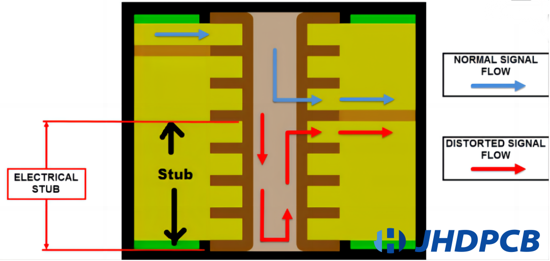
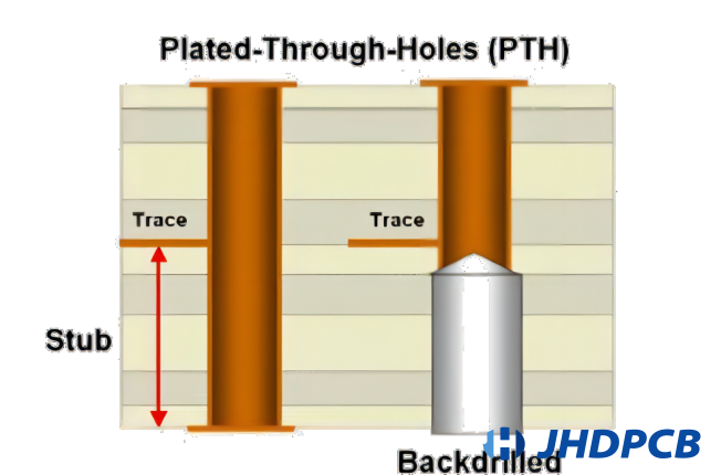
Backdrilling in multilayered printed wiring boards is the procedure of removing the stub to produce vias, allowing signals to move from one layer of the board to the next. (The stubs will create reflection, scattering, delay, and other issues during the signal’s transmission, which will cause the signal to be distorted.) Drilling at a controlled depth requires intricate skill.Making multilayer circuit boards, such 12-layer boards, requires connecting the first layer to the ninth layer. Typically, we drill through holes only once before plating the through vias. The first floor and the 12th floor are hence immediately connected. In actuality, the first floor just needs to be connected to the ninth floor. Since there are no wires linking the 10th through the 12th levels, they resemble pillars. This column has an impact on the signal path and may compromise the communication signal’s signal integrity. Therefore, a secondary hole was bored out of the opposite side of the extra column (referred to as STUB in the industry).

As a result, it is known as back drilling, however it is typically less clean than drilling because the next step will electrolyze some copper and the drill tip is also sharp. We will therefore leave a very small point; the length of this remaining STUB is known as the B value, and it typically ranges from 50 to 150 UM.

PTH

Back-drilling PCB technology

Due to the need to reduce signal loss for high frequency applications, a through hole connecting the layers is required for the signal to flow through as it moves from one to the other. It is recommended to remove the surplus copper from this hole for this application because it works as an antenna and affects the transmission if the signal is to flow from layer one to layer two in a 20 layer board, for example.

In order to gain greater signal stability, we drill out the “excess” copper in the hole using back-drilling (controlled depth in z-axis). The ideal outcome is for the stub (or “excess” copper) to be as short as possible. Typically, the back-drill size should be 0.2mm greater than the corresponding via.

BACK DRILLING (mm)  Parameters
A: Depth tolerance +/-0.10
B: Min. remain thickness and tolerance 0.15+/-0.1

Backdrilling PCB drill table

A placed drill table can be set up to display all drill layer pairs or a particular pair of layer pairs. In the image below, three tables have been assembled using a design that incorporates back drilling along the top and bottom borders of the board. The Drill Layer Pair column, which denotes the purpose of each table, should be noted.

Index Type Value min.
A Back drilling Ø 400µm
B Plated-through via Ø 200µm
C Copper clearance 150µm
D Ø-Difference circumference 100µm
E Back drilling depth 200µm
F Distance to connected layer see below
G Thickness target layer see below
H Thickness stub remainder (safety) see below

Required Target Layer Thickness“G

Please adhere to the following minimum prepreg thickness of the layer where drilling stops (G) if you require a particular layer buildup. We shall do the necessary thickness calculations for “G” in the absence of a particular layer buildup.

 F ≤ 1.0mm1.0mm < F ≤ 2.0mm2.0mm < F ≤ 3.0mm3.0mm<F≤
4.0mm
G min.250µm300µm400µm500µm
H125µm150µm200µm250µm
Tolerance± 100µm± 125µm± 175µm± 225µm

Key:
G min. = Thickness Target Layer.
H = Distance To Connected Layer.
Tolerance = Thickness Stub Remainder.

Back Drilling Examples

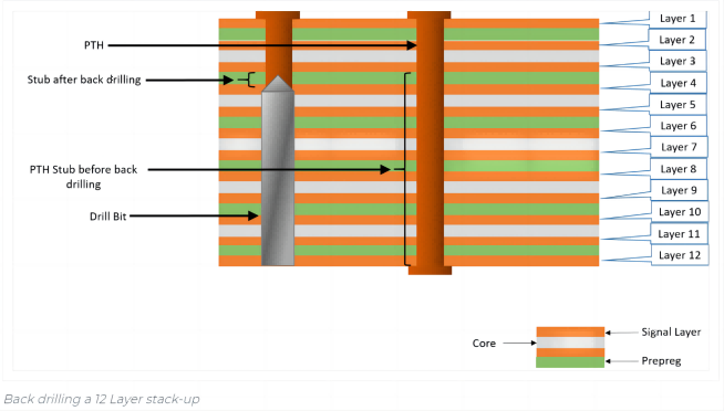
Consider a stack of 12 layers with a through-hole through running through layers 1 through 12. However, the through is only intended for layer 1 to layer 3 signals. So. After layers 3 to 12, a via stub will be produced, which will produce resonance and reflections at very high frequencies. The signals at the resonant frequency will be attenuated by it.In order to shorten the stub, back drilling is done to remove copper plating from layer 3 up to layer 12.The reverse drill needs to be larger than the initial hole size in order to remove the unwanted copper.

When building multi-layer circuit boards, such as 12-layer boards, we must connect layers 1 through 9. In most cases, we plate the through holes after one-shot drilling through the material.  This creates a direct connection between the first floor and the twelfth story. Actually, all that’s needed is a connection from the first floor to the ninth. It resembles a pillar since the 10th to 12th levels are not connected by cables. This column has an impact on the signal path and may compromise the communication signal’s signal integrity. Therefore, secondary drilling is used to drill an additional post, known as STUB in the industry.

back drilling 12 layers stack up

Back drilling from a manufacturing perspective

You should be aware that various construction techniques might potentially be used to shorten stubs. These include pcb back drilling laser vias (microvias), blind and buried vias, and pcb back drilling. Alternate stack-up arrangements, in which traces are moved to layers closer to the via stub, are also included. Additionally, back drilling is not required for high frequency (higher than 3CHz) boards since alternate methods of reducing signal reflection are employed instead.

However, from a production and cost perspective, these solutions aren’t always viable in many high-density PCBs and backplanes/midplanes. In these cases, the only choice is to remove the via stub by back drilling. When blind vias are not an option, back drilling is required for high frequency (more than 1GHz within 3CHz) boards.

Back Drilling or Controlled Depth Drilling in PCB

Back drill pcb

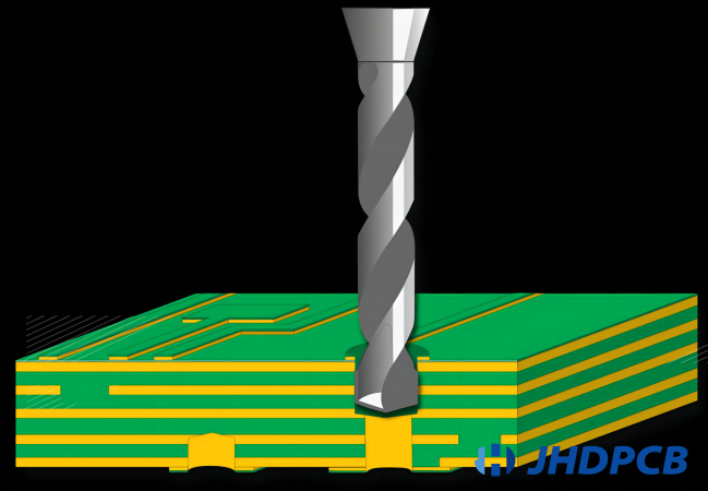
In order to retain the integrity of the signal on high-speed PCBs, there are various challenges that can be overcome by proper architecture and manufacturing procedures. In high-speed design, a transverse component, a non-functional component of a transmission, causes serious issues with signal integrity. Signals from the stub end are reflected through stubs, and this reflection distorts the initial signal. To counteract this, PCBs are routed using depth control, which involves redrilling with a slightly larger drill bit to remove the majority of the through stub.

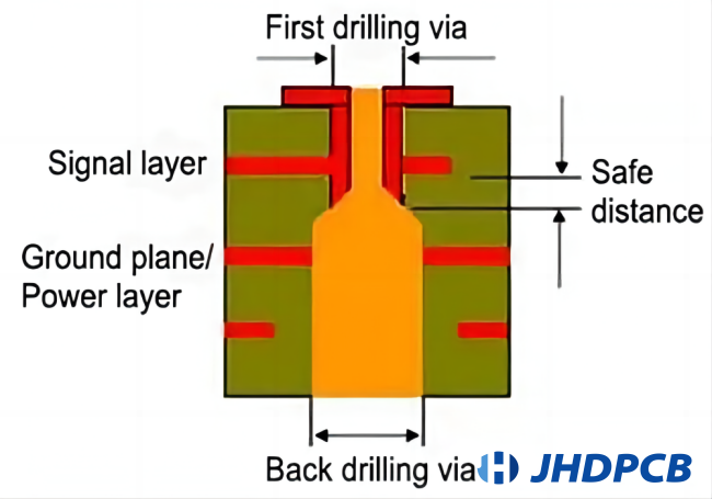
Drilling back is the process of removing the conductive from a stub by creating an opening only slightly larger than the PTH. The length of the stub should be cut in half, to 10 miles, by the back hole that was dug. Signal reflections are created if the stubs are more than 10 kilometers.

Electrical Connectivity with Back Drilling

Drilled through the PCB are thumbnail holes that provide electrical communication between the different PCB layers. The particular item demonstrates PCB back drilling via interconnected circuit board layers and their significance.

The part of a signal transmission that is not used is a back drill via stub. You may learn about stubs in and through them in this section. Stubs are signals that, especially for high-speed signals, cause a variety of signal integrity issues.

PCB assembly used through-hole technologies, including PCB through-holes, between the 1970s and the 1980s. It is still used today even though surface mounting technology is replacing it more and more. Through fissures, a plate (PTH) can become plated or unplated (NPTH). NPTH isn’t frequently used to assemble PCBs and install modules on the board.

Features of PCB back drilling.

Advantages of Back Drilling

  • Reduce noise interference & deterministic jitter;
  • Improve signal integrity;
  • Local thickness reduction;
  • Reduce the use of buried & blind vias and reduce the difficulty of PCB production;
  • Lower bit error rate (BER);
  • Less signal attenuation with improved impedance matching;
  • Minimal design and layout impact;
  • Increased channel bandwidth;
  • Increased data rates;
  • decreased EMI/EMC emissions from the stub end;
  • Reduced excitation of resonance modes;
  • Reduced via-to-via crosstalk;
  • Lower costs than sequential laminations.

Disadvantage of Back Drilling

High signals frequently have issues that might be linked to underutilized via stubs. Let’s take a closer look at a few of the problems with the stubs.

Jitter Deterministic:
Both clocks are timing, and the amount of time error is referred to as jitter. A deterrent jitter is what is known as a regular (i.e., limited) temporal modification.

Attenuation of the signal:
When a sound is attenuated, its intensity decreases and the pulse becomes weaker.

Radiation from EMI:
A via stub can be used as an antenna, radiating EMI.

General characteristics

  • Mostly are rigid boards on the back;
  • Normally used on 8 layers or above;
  • Board thickness is over 2.5mm;
  • Minimum hold size is 0.3mm;
  • Backdrill is 0.2mm larger than the vias;
  • Tolerance of backdrill depth+/-0.05MM.

What kind of PCB needs back drilling?

Typically, the PCB board holes are drilled through the board (from top to bottom). If the trace connecting the via holes is close to the top layer (or bottom layer), it will result in stub bifurcation at the via hole of the PCB interconnection link, which will affect the quality of the signal and cause reflections. Signals traveling at a faster pace are more affected by this effect.

In order to acquire a high quality of signal transmission, it is generally understood that the circuit track on the PCB board with its Signals at a rate of about 1Gbps needs to be considered to include back-drill design. Of course, designing high-speed connectivity lines requires system engineering and is not as straightforward as it may seem. If the system interconnection links are not too long or the chip’s drive capability is strong enough, the signal quality may be faultless without any back-drilling. Therefore, system interconnection link simulation is the most accurate method for determining if back-drill is required or not.

You may be aware that, in addition to using back drilling technology, various building methods can also be employed to reduce or optimize the length of the stub. These include different stack-up arrangements, where circuit track traces are shifted to layers closer to the end of the via stub, laser-drilled vias (microvias) holes, or blind and buried vias. Additionally, as other methods are employed to lessen signal reflection on high frequency (higher than 3GHz) boards, back-drilling is not required.

However, these approaches are not always practical from a manufacturing facility and cost standpoints to reduce the signal loss in many high-density PCBs or backplanes/mid-planes. So, the only practical choice is to back drill the via stub out. When blind vias holes are not an option, back drilling becomes imperative for high frequency (more than 1GHz inside 3GHz) boards.

And since the PCB has so many layers, some holes cannot be designed as blind holes (for instance, on a 16-layer PCB, some via holes must connect to layers 1 through 10 and another via hole must connect to layers 7 through 16; this design is not suitable for blind holes but is suitable for back drilling).

How to do PCB back drilling?

How to do PCB back drilling

The Process of Back Drilling
  1. To locate the first drilling hole, use the positioning hole on the PCB that is provided.
  2. Before plating, use dry membrane to seal the position hole.
  3. Powder the hole with copper to create a guide circuit.
  4. Create an outer graphic on the PCB.
  5. After creating an outer layer pattern, the graphic board will be executed on the PCB. Before this process,It is crucial to seal the placement hole with a dry membrane before beginning this process.
  6. Use the first drilling’s placement holes to align the back drilling, then use the drill bit to drill the electroplated holes that call for this procedure.
  7. After the final drilling, the board needs to be cleaned in order to get rid of any potential leftover drills
  8. After the board has been validated and the signal integrity has been improved, pay close attention to whether the drilling operation is being carried out appropriately.
Test the Back Drills

Once the routing is finished, we must ensure that the back drills have been set up properly. To validate this, turn on all layers. You’ll see that the vias’ rim has two colors on it. The first or the starting layer is shown in red, while the final layer is shown in blue. It is simple to tell the back-drilled vias apart from the other vias. Only the back drilled vias are visible with two colors.

Click Drill Table after selecting the location from the main menu to find out how many Vias, PTH, and other trolls have been carried out.

Technical difficulties of back drilling process.

  1. Back drilling depth control 
    For accurate processing of blind vias, back drilling depth control is crucial. The back drilling depth tolerance is largely influenced by the back drilling equipment’s precision and the medium thickness tolerance. Back drilling accuracy, however, can also be impacted by outside variables such drill resistance, drill tip angle, contact effect between cover board and measurement device, and board warpage. To get the greatest results and manage the accuracy of back drilling, it’s crucial to choose the right drilling materials and techniques during production. Designers can guarantee high-quality signal transmission and avoid signal integrity problems by meticulously managing the depth of back drilling.
  2. Back drilling accuracy contro 
    Accurate back drilling control is crucial for the quality control of PCB in subsequent processes. Back drilling entails secondary drilling based on the initial drill’s hole diameter, and secondary drilling precision is crucial. The precision of the secondary drilling coincidence can be impacted by a number of variables, such as board expansion and contraction, machine accuracy, and drilling techniques. It is essential to make sure that the back drilling procedure is precisely controlled drilling in order to minimize errors and maintain ideal signal transmission and integrity. 

Back drilling PCB design considerations.

It is essential to give PCB board manufacturers separate output files containing the back diamond layer and to explicitly state which layer calls for the associated back diamond specs in order to secure the correct back diamond. The back drill’s diameter needs to be at least 0.2mm bigger than the first drill’s diameter. In the first drilling hole, there should be a 0.2mm drilling and a 0.35mm separation between the wiring and the back drilling layer. To prevent drilling wiring that shouldn’t be drilled, the thickness of the electrical media should be taken into account when constructing the PCB layer. It is not necessary to drill at least 0.2mm of the medium between the adjacent layer of drilling and the “L” layer if only the specific layer—for instance, the “L” layer—needs to be done.

A little wider than the primary drilling diameter is required for the PCB rear drill. The back pin typically has a diameter of 8 mils over the size of the main pin, with a recommended length of 10 mils. Authorizations for traces and planes need to be robust enough to stop unintentional back drilling in traces and planes adjacent to the backboard hole. It is preferred that airplane and trace (space) clearances have a minimum of 10 miles.

Additionally, fewer over-hole piles and fewer blind holes must be avoided in order to maximize the back diamond technology. Signal reflection and other issues can be avoided by retaining the minimal distance between signal wiring and back drilling and inserting perforated material in less important regions. It’s crucial to maintain a smaller rear drilling diameter to prevent wiring and plane from entering the back plate hole.

Additionally, taking back diamonds into account from the initial design phase can assist guarantee that the essential measures are taken to maximize signal integrity and avoid issues throughout the manufacturing process.

How much remaining stub length can the backdrill retain?

You must calculate the amount of residual stub length that won’t harm your PCB before back drilling. However, choosing this factor will depend on a number of factors, such as your preferred signal integrity and real-world manufacturing techniques. 

Usually, lowering the maximum length of a leftover stub and raising the Vias for back-drilling will raise the cost of production. 

The following table shows the remaining stub length and related signal loss.

Residual Stub Length (mils) Residual Stub Length (mils)
200 50%
100 25%
60 15%
40 10%
20 5%
10 2.5%
5 1.25%
2 0.5%
1 0.25%

Duration of stub residual

You must choose how much stub duration is left if you have decided to return to the drill. The choice is based on a number of interconnected factors, including the best signal integrity output and practical (cost-effective) production concerns and constraints. Costs associated with PCB/backplane fabrication would typically increase if more drilled vias were used and the total residual stub lifetime was shortened.

FAQ of Back dirlling

Back drilling is also known as controlled depth drilling since these holes are back drilled to a predetermined, regulated depth. 

Traces may be transferred to layers that are closer to the end of the via stub using different stack-up arrangements, such as laser-drilled vias (microvias), blind and buried vias, and so on.

It is more difficult to minimize stub length below 10 mil since it requires the drill machine to be more accurate. Additionally, it raises manufacturing costs, making it challenging to shorten stubs. There is a chance of getting 2 to 3 mil stubs if your manufacturer uses the most recent drilling technology. Consult the manufacturer.

More drill machine accuracy is needed for back drilling below ten mils. And trying it is really difficult. Additionally, decreasing below 10 mils raises the cost of production.

The most important and challenging step is drilling because even a slight error might result in significant damage. Before placing an order, you should consider the PCB maker’s skills. JHD PCB offers back drilled boards at affordable pricing and specializes in PCB prototype assembly. Our benefits include quick delivery times and high reliability. JHD PCB, a well-known PCB manufacturer in China, has all the knowledge and abilities required to assist you. If you have any suggestions for a PCB assembly or prototype, please contact us

Get a PCB Quote Now

Open high-quality PCB manufacturing services in JHDPCB

Leave a Comment