PCB In-Circuit Testing

In-Circuit Testing (ICT): Pros, Cons and Detecting Defects

directory

Printed Circuit Boards (PCBs) form the backbone of modern electronic devices, enabling the seamless flow of signals and power between components. Ensuring the reliability and functionality of these intricate circuit boards is paramount in the electronics industry. In-Circuit Testing (ICT) has emerged as a powerful and indispensable tool in the PCB manufacturing process, providing a comprehensive evaluation of the electrical integrity and performance of the assembled PCBs. At JHDPCB, we are dedicated to utilizing advanced ICT techniques to deliver high-quality PCBs that meet the stringent standards of our clients.
In-Circuit Testing revolutionizes the testing process by examining the individual components and connections within the PCB. By using specialized test probes, ICT assesses the electrical continuity, verifies component values, and identifies potential defects or faults. This method allows for the detection of issues such as short circuits, open circuits, incorrect component values, and manufacturing defects. Through ICT, we can identify and rectify these issues during the manufacturing process, ensuring that the final PCBs meet the highest standards of performance and reliability.
At JHDPCB, we recognize the critical role of ICT in guaranteeing the quality of our PCBs. With our state-of-the-art facilities and skilled technicians, we conduct thorough and accurate ICT to assess the functionality and electrical characteristics of our assembled boards. Our commitment to excellence extends to the implementation of advanced testing equipment and stringent quality control measures, ensuring that our clients receive PCBs that meet their precise specifications and requirements.
In this article, we will delve deeper into the world of In-Circuit Testing, exploring its advantages, working principles, and the vital role it plays in the PCB manufacturing process. We will showcase JHDPCB’s expertise in incorporating ICT into our manufacturing workflow, emphasizing our commitment to delivering reliable and high-performance PCB solutions to our valued clients.
Join us as we embark on an informative journey through the intricacies of In-Circuit Testing, discovering its immense value in the electronics industry and how JHDPCB’s capabilities ensure superior PCB testing and quality assurance.

What is In-Circuit Testing (ICT)?

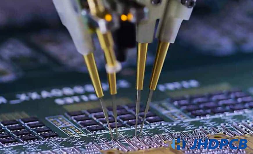
In-Circuit Testing (ICT) is an automated test method used to verify the quality and functionality of electronic assemblies. ICT involves the application of test signals to components on a live circuit board to detect any manufacturing defects. It is often used as a final quality check of printed circuit board assemblies (PCBAs) before the boards are shipped to customers or moved to the next stage of production.

ICT testing is performed using dedicated testing equipment known as In-Circuit Testers. These testers have spring-loaded pin probes that make contact with test points on the PCB to apply test signals to components. The test signals stimulate the components and the tester verifies if their responses match the expected values to determine if the components and circuit paths are functioning correctly. In addition, testers can also check components such as resistors, capacitors, diodes, and integrated circuits. They can also perform checks such as shorts, opens, tolerance, and continuity tests across the board.

PCB Testing-in-circuit testing

Some key benefits of ICT are that it can detect up to 99% of manufacturing defects, which leads to improved quality and reliability of the PCBA. It also helps reduce rework and repair costs. ICT is very fast since many tests are executed in parallel, and it does not require powering up the entire board.
Moreover, the test coverage of ICT can include Boundary Scan testing, analog signature analysis, and parametric tests. Boundary Scan uses built-in test logic in ICs to control and observe other devices on the board. Analog signature analysis injects a signal and captures the response to check for deviations. Parametric tests measure key attributes like resistance or capacitance to ensure components are within tolerance.
Overall, ICT is a highly efficient method for verifying PCBAs by detecting manufacturing defects prior to assembling the boards into final products or systems. When implemented as part of a robust quality management process, ICT can help achieve high yields, reduced failures, and quality electronic products.

Characteristics of In-Circuit Testing.

In-circuit testing (ICT) is a widely used and reliable method of testing printed circuit boards (PCBs) for manufacturing defects. Like any testing method, there are advantages and disadvantages to consider when determining the best option for a particular application.

Advantages of In-Circuit Testing:

  • ICT is a fast and accurate method of testing that can quickly detect defects in components, continuity, and other faults.
  • The operation is simple and user-friendly, leaving little room for error.
  • With a testing time of usually 1-2 minutes per assembly, ICT is ideal for larger volumes of production.
  • In-Circuit Test Programming is a comprehensive and reliable testing method that provides high fault coverage for manufacturing defects.
  • Test results are easy to interpret and understand.
  • This testing method is particularly well-suited for medium to high-volume through-hole PCBAs.
  • Minimal maintenance costs are required, making it a cost-effective option.
  • ICT can be easily integrated into an automated production line, increasing overall efficiency.
  • The test procedure can be easily updated and modified, making it suitable for various PCB designs and technologies.
  • ICT helps in reducing the risk of field failures and ensuring high-quality end product.

Disadvantages of In-Circuit Testing:

  • In-circuit test fixtures can be expensive to create and develop, particularly for low-volume production.
  • In high-density, small package size surface-mount technology (SMT) components, ICT may not always identify connector faults.
  • Proper contact between the test pins and the corresponding test pads is crucial to obtain consistent results using In-Circuit Test Programming. Otherwise, inconsistent result can occur.
  • Failing to clean or replace test pins regularly may result in failures and false calls, which can affect the accuracy of the testing process.
  • Limited access to test points on densely populated PCBs can make ICT challenging or impossible to implement.
  • Creating ICT test programs can be a time-consuming process, especially for intricate designs.
  • ICT is focused on detecting manufacturing defects, but may not be as effective in identifying design or functional issues.
  • The test fixture and programs may need to be redesigned for each new board revision, increasing the overall cost and lead time.
  • ICT can be less effective in detecting intermittent faults, which may only occur under specific conditions.
  • Some components, such as sensitive analog circuits and high-speed digital designs, may be adversely affected by the test procedure, leading to false failures or damage to the components.

Despite its limitations, ICT is a reliable and widely used testing method that can provide manufacturers with the confidence that their PCBs meet the required quality standards.

What Defects Can ICT Detect in PCBs?

So, now in this section, we will introduce some of the defects that ICT can identify;

  • Shorts between component leads and traces;
  • Solder bridges;
  • Short circuits;
  • Component markings;
  • Soldering and process issues;
  • Lead spacing, component spacing, land, and component sizes;
  • Resistor values in the circuit;
  • Correct location/setting of switches or jumpers;
  • Presence or absence of passive elements;
  • Presence or absence of active analog elements;
  • Misoriented analog components;
  • Misoriented digital elements;
  • Inductance and capacitance values;
  • Missing or wrong components;

It is important to keep in mind that In-Circuit Test Programming has certain limitations. For instance, it may not be able to identify missing multiple power connections, mechanical fixings, decoupling capacitors, and other design-related issues.

What are the Common Types of ICT Testers?

There are several types of in-circuit testers used for printed circuit board testing:

  1. Standard ICT: A traditional ICT system uses fixed pin probes that contact test points on the PCB to check for defects. It provides basic test coverage at a low cost but requires test points to be incorporated into the board design.
  2. Flying probe tester:This uses movable probes that can access components without fixed test points. It offers greater flexibility and test access but at a higher cost. Flying probe testers are ideal for boards where access to testing points is challenging.
  3. Manufacturing Defect Analyzer (MDA):An MDA uses non-contact probing to detect manufacturing and design defects. It uses electromagnetic sensors to check for issues like incorrect components, soldering defects, and track/land faults. MDAs provide fast, comprehensive testing without requiring test points but have higher upfront costs.
  4. Cableform tester: For flexible or rigid-flex PCBs, a cable form tester is used. It has motorized probes to access both sides of the PCB and check for defects specific to flex circuits like conductor exposure or breaks. Cableform testers provide specialized testing for flex PCBs at a relatively higher cost.

To choose the appropriate ICT system, several factors must be considered:

  • PCB complexity and density: Complex boards with limited test access require more advanced flying probes or MDA testers. Simple boards can use standard ICT.
  • Test coverage required: To detect a wide range of potential defects, MDAs provide the highest test coverage. Standard ICT offers basic coverage.
  • Volume and cost: For high-volume production, standard ICT is typically the most cost-effective. MDAs and flying probe testers are better for lower-volume, higher-quality testing.
  • Flexibility:Flying probe testers offer the greatest flexibility to test hard-to-reach components. Standard ICT requires predefined test points.
  • Available test access:The number and location of test points should guide the choice between a standard ICT system or a flying probe/MDA tester.

What are the components to perform the In-Circuit Testing?

To make informed decisions about in-circuit testing, it’s essential for engineers to understand the various types of in-circuit test systems available in the market. To ensure the production of the best possible final product at the most optimal cost, it is essential for engineers to understand the differences in performance, capability, and procedure among various testers. By doing so, they can select the most suitable tester for their needs.
All in-circuit testers share some common elements, including:

  1. Software:The software controls the testing process and analyzes the results, identifying any faults or defects in the PCB’s components.
  2. Controller:The controller manages the tester’s functions and interfaces with the software and the fixture.
  3. Fixture: The fixture is a custom-designed interface that connects the tester to the PCB’s test points.
  4. Interface: The interface connects the fixture to the tester and provides a means for the tester to apply the correct voltage and signal to the PCB’s components.
  5. Powered Analog Tests: These tests apply a voltage or current to a component and measure its response, allowing for the testing of analog components.
  6. Analog Scanner: The scanner can test multiple analog components simultaneously, improving testing efficiency.
  7. Analog Digital Opens: These tests measure the resistance between a component’s pins, allowing for the testing of digital components.

There are various types of in-circuit testers available, including flying probe testers, bed-of-nails fixtures, bed-of-nails testers, and hybrid testers. Different types of testers have their own distinct features and advantages, making them suitable for various PCB types and production volumes.

Flying Probe Test vs ICT Test: A Comprehensive Comparison.

When it comes to testing the functionality and integrity of printed circuit boards (PCBs), our customers often don’t know how to choose between flying probe testing (FPT) and in-circuit testing (ICT). Below, we will comprehensively compare the characteristics and applications of FPT and ICT. By understanding the differences and advantages of each inspection method, you can make an informed decision about which test method is best for your specific PCB manufacturing needs. Join JHD for a deep dive into the world of FPT and ICT, examine their main characteristics and explore factors to consider when choosing the most appropriate testing strategy for your PCB project.

CriteriaFlying Probe TestIn-Circuit Testing (ICT)
Test MethodNon-contact, uses probes to test points on PCBContact, uses a custom fixture to test components in-circuit
Setup TimeQuick and automated, no custom fixtures requiredTime-consuming due to custom fixture development
CostLower upfront cost, suitable for low to medium volume productionHigher upfront cost, suitable for high-volume production
Test CoverageLimited coverage, cannot test components under ICs or in hard-to-reach areasComprehensive coverage, can test most components on the PCB
Fault DetectionCan detect open circuits, short circuits, and component valuesCan detect the same faults as Flying Probe Test, as well as additional faults such as missing components
SpeedFaster for small to medium volume runsSlower for small to medium volume runs, but faster for high-volume production
FlexibilityMore flexible, can be easily modified for different PCB designsLess flexible, requires custom fixture development for each PCB design
AccuracyHigh accuracy for small to medium volume runsHigh accuracy for all production volumes
ReliabilityReliable, with low risk of damaging componentsReliable, with low risk of damaging components
ApplicationsSuitable for low to medium volume production runs and prototypesSuitable for high-volume production runs and complex PCBs

So, that was all about in-circuit testing and flying probe tests. In-circuit testing (ICT) and Flying Probe Test (FPT) are two powerful testing methods that can help manufacturers maximize efficiency in PCB testing. By utilizing these testing methods, manufacturers can ensure that their PCBs meet the required quality standards and function correctly and reliably.

At JHDPCB, we understand the importance of quality testing in PCB manufacturing. We offer a range of testing services, including ICT and FPT, to ensure that our customers receive high-quality PCBs that meet their requirements. Our experienced engineers use state-of-the-art equipment and software to perform comprehensive testing, providing our customers with the confidence that their PCBs will function correctly and reliably.
FPT is usually used in small quantities order, and ICT requires custom fixture development for each PCB design, and such fixtures are usually paid by the customer and can be reused in each production batch. Of course, we can support free fixtures to do E-testing in big quantities order.

We recommend JHDPCB as a reliable and trusted partner for all your PCB manufacturing needs. With our commitment to quality, competitive pricing, and excellent customer service, we can help you deliver high-quality products to your customers and stay ahead of the competition.

Get a PCB Quote Now

Open high-quality PCB manufacturing services in JHDPCB

Leave a Comment