PWB VS PCB: Differences and In-Depth Guide.

directory

What is PWB?

A PWB is a board that is used to mount and connect components. In order to create an electronic circuit that works, it is used to provide interconnections and component attachment bases. A PWB becomes a printed wiring assembly (PWA), which is the same as a printed circuit assembly once all of its electrical components are joined (PCA).
The name PWB was used in the early phases of electronics manufacturing when using surface mount technology and the circuit only had a point-to-point connection. The gradual move to PCB occurred as development reached the point where conductors could run from one side or layer of the board to the next, offering enhanced functionality.

What is a PCB?

Copper conductors are used to providing electrical connections between parts of an electronic assembly called a printed circuit board (PCB). For the purpose of mounting the gadget in an enclosure, the PCB offers mechanical support for the electronic components. A precise set of actions that are in line with the manufacturing procedure, the integrated circuit package, and the structure of the bare circuit board must be included in the design of a printed circuit board.
Click to view the detailed PCB manufacturing process;
Click to view detailed PCB package introduction;
Copper traces, pads, and conductive planes are examples of the conductive components on a printed circuit board. An insulating material is layered between the conductor layers to form the mechanical structure. To provide a legend for the electronic components, screen-printed material is printed on the solder resist layer, which is coated with a non-conductive solder resist layer and plated over the entire structure. The bare board is shipped to the printed circuit board for assembly, the components are soldered to the board, and the PCBA is ready for testing after these manufacturing stages are finished.

PCBs are crucial because they provide electrical connections between components, rigid supports to keep components in place, and small packages that may be integrated into the finished product. Printed circuit board design has grown into a vertical within the electronics industry.

What is the difference between PWB vs PCB?

Circuit boards comprised of one or more layers of copper laminated to a non-conductive plastic sheet that holds and links components with conductive tracks are referred to as PCBs and PWBs, respectively. However, there are some distinctions between them because PWB refers to the first varieties of printing circuit boards before the developments in circuit technology that led to their creation. In the early days of the electronics industry, circuit boards had few connections, which made the phrase “printed wiring board” the perfect fit for them. PWBs serve as the foundation for PCBs, which are an upgraded word for circuit boards with superior technology. PWBs and PCBs are exactly like computer programs and software, which can be updated while effectively maintaining compatibility with earlier versions. The similarity arises from the fact that the only things separating them since their creation are the changes that have occurred.

When electronics were first developed, the phrase “printed wiring board” was used. Because the connections on the board were just from one point to another, it was thought suitable to use the moniker PWB in the early days of the industry as a whole.
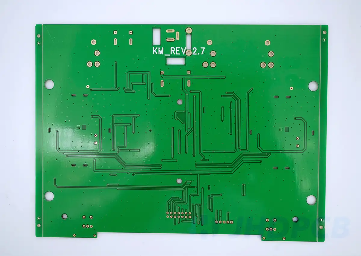
A PWB is a design substrate that has no installed components. The PWB contains apertures for soldering electronic components in addition to the etching drill. Before being converted into a PCB, the PWB must go through a number of chemical and physical processes in addition to installing the electrical components. this is due to the fact that the functionality of the course is greatly influenced by the printed circuit board’s design.
Later, when circuit board technology advanced, the compound word “printed circuit board” was coined. At first, the compound term could only be used internally; the word “circuit” was more appropriate because printer circuit boards allowed more sophisticated capabilities. PWBs are becoming less common in the pre-production of electronic items as a result of the advancement of technology and the widespread adoption of the word PCB.
As printed circuit design frequently affects functionality, the IPC Technical Activities Executive Committee authorized the usage of the term PCB only in all new document creation about 1999.

PWBs and PCBs also differ from region to region. For instance, the term printed circuit board is more frequently used in the United States, whereas PWB is more frequently used in Japan. Because it avoids confusion with the other word PCB, which refers to a specific poison available in Japan, PWB is chosen over PCB in that country.

What other terms are there for printed circuit boards?

PCB (Printed Circuit Board), often known as the printed circuit board, is a crucial electronic component that serves as both the carrier for electrical connections between electronic components and the support body for those components. It is referred to as a “printed” circuit board since electronic printing technology was used to create it. This is the most commonly used board designation inside JHD.

The term “PCBA” stands for “Printed Circuit Board +Assembly,” which refers to the entire process of assembling a PCB air board after SMTing its component elements and before the DIP plug-in. In contrast to the normal form of writing in Europe and North America, which is PCB’A with the addition of “‘,” which is known as the official idiom, this is the way that is frequently used in China.

Print on a board. A bare board’s most general designation.

A printed board is a PWB. A PWB also referred to as a PCB, is a board on which parts are attached and connected.

Printed wiring assemblies are known as PWAs. When a PWB’s electrical components are entirely connected, this phrase is frequently used to describe it.

Printed circuit assembly is known as PCA. Printed circuit boards that contain electronic components are known as PCAs. The presence of electronic components defines a PCA. The board is nothing more than a PCB without these parts mounted.

A PCB having electrically and physically connected electronic components is referred to as a “circuit card assembly.”

Which materials are used in PWB and PCB manufacturing?

Due to the similar design, the PWB and PCB can be made from similar materials. PWB and PCB may also use different materials depending on how the board is applied. In these kinds of boards, there are conductive and non-conductive layers. Galvanic isolation is normally achieved using the non-conductive layer, whereas signal transmission is typically achieved using the conductive layer.

  • Conductive layer material: Conductive layers are utilized to build signal transmission paths on PWBs and PCBs. For conductive layers, common PCB materials include copper, silver, and gold.
    Although gold has the highest electrical conductivity and the lowest resistance, its use is limited by its high price. Copper is the preferred material for most PWB and PCB applications due to its benefits, which include its low cost and better conductivity.
  • Substrate material: The non-conductive layer is composed of an ineffective electrical transmission material. This layer is constructed from ceramics, FR-4, and composite epoxy resin components. These materials have different heat conductivities and insulating properties. To enhance its dielectric properties, FR-4 is frequently used in a variety of configurations. More PCB substrate types can be learned through our related blogs.
  • Prepreg: Another substance that is widely utilized in PWBs and PCBs is prepreg. Prepreg is used to hold layers together, like in the core of a board. It is constructed from glass fiber that has previously undergone resin treatment. It becomes pliable at high temperatures and adheres to the layer’s surface; as it cools, it solidifies and forms a bond.

Other materials, such as solder, are also found on these boards. The essential ingredients in solder, which is commonly used for component connections, are lead and tin. To prevent corrosion from substances like gold, nickel, silver, and tin, the conductive traces can also be coated.

What surface finishes can be applied to PWB or PCB?

Surface treatments are protective coatings used on the trace patterns of printed circuit boards. Ensuring good solderability or electrical characteristics is the primary goal. You will discover that applying a surface treatment to copper traces can both stop corrosion and enhance the board’s solderability.
As for finishes, you have a variety of choices, including immersion tin and immersion silver, HASL and ENIG. Metal surface molding includes both immersion tin and immersion gold. Your choice of surface finish will be influenced by a number of variables, including:

  • The price of putting the finish to the surface.
  • Board dimensions and overall board count.
  • The board is filled with data and has the corresponding attributes.
  • A surface finish’s level of durability.

There are various methods for treating PCB surfaces. Processes used to treat surfaces might be either metallic or organic. OSP pertains to organic surface molding, whereas HASL, ENIG/ENEPIG, immersion gold, and immersion tin all belong to metal surface molding. More detailed surface treatment process can be learned through JHD blog.

PWB Manufacturing Methods and Types.

PWB manufacturing metho:

PWBs are divided into two varieties based on the production process. These operations involve addition and subtraction. To produce the circuit, subtractive processing entails carefully removing copper from the PWB. Other metals are added by manufacturers during the plating procedure. The usage of image transfer from the image file to the copper circuitry on the board is referred to as subtractive processing.
Manufacturers use the additive processing technique to add copper to produce a picture. There is no etching or copper removal during this operation. PWBs have been created via additive manufacturing for many years.

Classification of PWBs:

  • PWBs can be categorized in several ways. Printed wire boards are divided into rigid boards, PKG boards, flexible printed circuit boards, build-up and LED boards based on their shape and intended usage.
    The substrates used in flexible PWBs include polyester and polyimide. These boards are still adaptable and perfect for many different kinds of applications. It is possible to repeatedly bend a flexible PWB. PWBs can endure numerous flex cycles.
    Rigid PWBs are the most common circuit board subtype. The board is made by manufacturers using glass-reinforced epoxy. Less than 0.1 inches thick describes rigid PWBs. Both rigid and flexible qualities can be found in rigid-flexible circuit boards.
  • The industry also classifies them according to the number of layers of the board’s total complexity. PWBs are divided into three groups based on the number of layers: single-sided, double-sided, and multilayer.
    A multilayer PWB has circuitry on more than two layers. This indicates that the substrate beneath the board’s surface has at least one layer. As many interconnected layers as possible may be present in a multilayer PWB. The most popular ones, though, are 4, 6, and 8 layers. Only two interconnected layers are present in double-sided PWBs. Compared to multilayer boards, this sort of PWB is more simpler to construct. A layer of circuitry is present on the single-sided printed wiring board.

What factors determine printed wire board performance?

The performance of the finished product is based on the PWB structure’s quality. When creating printed wiring boards for their PCBs, PCB designers and assemblers must take into account a variety of elements. These consist of:

The circuit built on the PWB will, in the finished product, enable electricity to flow from the power supply through the traces to the component and back again. The board’s copper wires are primarily responsible for this.

  • Signal strength and speed are impacted by the substrate nearby. It is mathematically inversely related to the substrate material’s square root dielectric constant. In simple terms, the signal encounters higher resistance the thicker and less conductive it is.
  • The flight time of a signal is also influenced by the conductor’s length. Shorter conductors must be used by assemblers to produce a tidy and quick design. Stripline and microstrip can complement conductors for better performance if performance above 25MHz is necessary.
  • Copper thickness is another element that influences signal propagation. The overall thickness of the PWB is influenced by copper thickness. The amount of current that must flow through the PCB typically determines the thickness of the copper layer utilized. The typical thickness of copper is between 1.4 and 2.8 mils (1 and 2 ounce), but this thickness might vary depending on the specific needs of the board. Due to material requirements and production difficulties, thicker copper will result in thicker pwb boards and higher board prices.

When creating printed circuit board assemblies, power consumption is a constant worry, and issues might arise at the PWB stage. Power consumption grows along with the number of circuit gates. The ideal power supply must be taken into account while constructing a PWB, and the number of gates and clock rate must be adjusted correspondingly.
Additionally, while designing high-speed switching circuits, you must account for the traces’ ground return current. Switching circuits can easily produce overheating, burnout, or a halt in the flow of electricity if the ground levels are incorrect.
To keep resistance low in the case of multilayer boards, a ground plane is required between each layer. These will efficiently disperse the return current and serve as a larger ground area.

Heat is inefficiently conducted by the PWB itself. Because the substrate absorbs and retains heat, extra mechanisms for releasing heat must be incorporated into the PWB. High-speed circuits require more advanced thermal management capabilities, even though FR4 is the optimum material for most circuits because it can dissipate heat quite well. Thankfully, there are approaches to accomplish this. You can use them:

Heatsinks: Heatsinks are intended to remove heat from the board so that it can dissipate without damaging the electronics.
Thermal vias: Sometimes referred to as thermal vias, are tiny holes surrounded by conductive materials that allow heat to pass through the circuit board.
Thermal Pad: It is a layer of conductive material, often used with multilayer boards. They can transfer heat from the inside of the board to the outside while providing a larger area to safely dissipate the heat.

Any of these building blocks can be included in the structure of the PWB to improve thermal management, component utilization and current flow. The design and number of layers of the PWB will affect the choice of method. You can choose a suitable method for thermal management according to the actual situation. The design of the PWB is as important, if not more important, than the overall strategy of the product. A poorly designed PWB can produce a defective finished product. Therefore, considering heat dissipation in the early stage of design can reduce a lot of unnecessary troubles.

PWBs are employed in numerous distinctive ways across a range of sectors. You must ascertain and incorporate into your design the needs of your application. This is critical for calculating trace copper thickness. Depending on the application area, the present needs are a key factor for PWBs.

Estimating expenses is essential for any design job, especially if there are financial constraints. The intricacy of a printed circuit board raises the price of the board. A multilayer board layout, for instance, will cost more than a single board.

Common components mounted on PWBs.

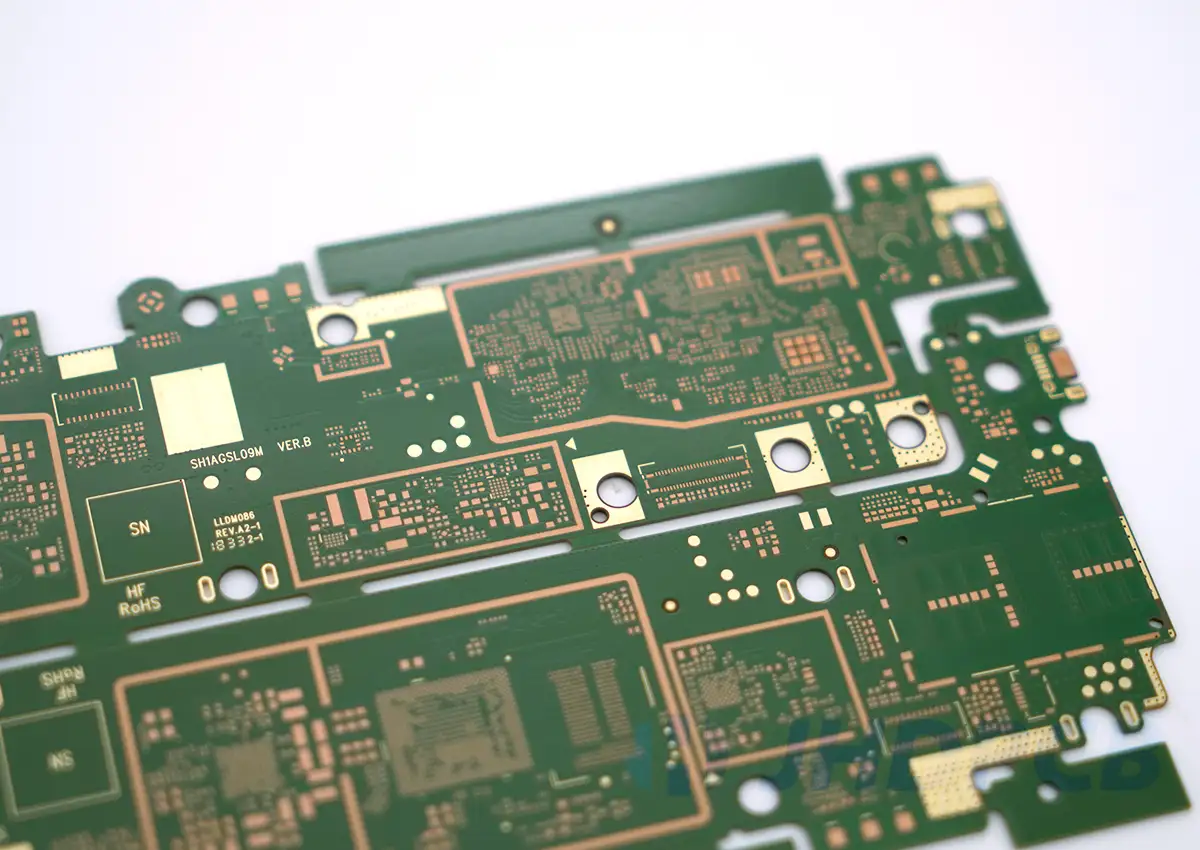
PWB assembly includes a number of electronic parts. In addition, producers mount these parts on PWB-printed wiring boards. Among the elements of a PWA are:

  • Resistor.
    By turning electrical energy into heat, they serve the purpose of halting electrical current. The “axial” style resistors, which have leads at both long ends and colored rings engraved on the body, are the traditional resistors that hobbyists are most familiar with. They come in a variety of varieties and are constructed from a variety of different materials. These rings serve as codes for the resistance values they represent.
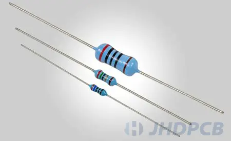
    Resistor

  • Capacitor.
    A capacitor’s job is to briefly store a charge before releasing it when another part of the circuit requires more power. Usually, it accomplishes this by accumulating opposing charges on two conducting layers that are separated from one another by an insulating or dielectric substance. Capacitors are often categorized based on the conductor or dielectric material. This leads to a large variety of capacitor types with distinct properties, ranging from high capacitance electrolytic capacitors to diverse polymer capacitors to the more reliable ceramic disc capacitors. While some look like axial resistors, traditional capacitors are radial in design with both leads sticking out of the same end.
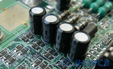
    Capacitor

  • Inductor.
    Along with resistors and capacitors, inductors are the final linear passive component in the chain. Like capacitors, they also serve as energy storage devices, but inductors do so by storing energy in the form of the magnetic field that is produced as current passes through them. Uncomplicated inductors are coils. The magnetic field and inductance increase with the number of windings. They might be coiled on various core shapes. As a result, the magnetic field and hence the stored energy are amplified greatly. Inductors are frequently employed to filter or block certain signals, such as in radio equipment to prevent interference, or in switch-mode power supplies to control AC signals along with capacitors.
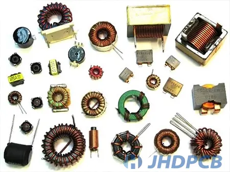
    Inductor

  • Diodes.
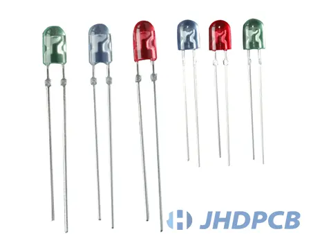
    A diode is a component that only permits electricity to flow in one direction, from the anode (+) to the cathode, much like a one-way street (-). This is accomplished by the resistance being strong in one direction and zero in the other. This function can be used to prevent damaging currents from flowing in the wrong direction. Light-emitting diodes, or LEDs, are the most well-liked diodes among amateurs. As their name implies, they are used to emit light, but anyone who has soldered before understands that they are actually diodes, so be careful to pay attention to the direction; otherwise, the LED won’t light up.

    Diodes

PWB Assembly Process.

There are several steps in the PWB assembly process. Manufacturers must carefully complete these steps to produce a PWB assembly that functions. It’s crucial that you properly integrate each of these steps. Additionally, you must take into account the input results to output outcomes at every level. This will assist you in maintaining quality while you assemble PWBs. Additionally, you would be able to spot mistakes early on and fix them.

  • Solder paste:
    The initial stage of a PWB assembly is this. All places that need soldering receive a solder paste addition from the manufacturer. This must be completed prior to attaching the components to the PWB. The locations that require solder paste are the component pads. Flux and solder granules are combined to form the solder paste.
    The solder screen is placed on the PWB by the assembler. Through the holes on the board, a runner passes through the screen and applies solder paste to the screen. To guarantee that the junctions have the proper amount, the assembler must regulate the amount of solder paste.
  • Component placement:
    This step in the PWB assembly process is crucial. Component placement on the PWB is done at this step. On the PWB, the electronic parts are mounted. Here, the component is soldered to the board’s surface by the manufacturers. This method was manual back then. Tweezers are used by assemblers to select and position parts on the PWB. But many things have improved thanks to technology.
    PWB assemblers now pick and place components automatically using a machine. On top of the solder paste, the machine automatically installs electronic components in predetermined locations.
  • Reflow soldering:
    Solder paste must set up in this situation. In actuality, the attached components and solder paste must stay in place. This is done by the PWB assembler using “reflow.” The board is transferred to a conveyor belt by the assembler once the components have been placed. This belt travels within the reflow oven. The oven resembles a professional pizza oven.
    The reflow oven includes a number of heaters. These heaters bring the pwb circuit board’s temperature to the proper level. This stage sees the solder paste melting. The cold heaters then solidify the solder by cooling it down as it passes through them.
  • Inspection and test:
    It may take some time to inspect a PWB, but the effort is worthwhile. You must inspect the board once the assembling procedures are completely finished. You can find any flaw or mistake in the PWB assembly by performing a thorough check. On the printed circuit board assembly, an automatic optical inspection can be done. This procedure finds damaged joints, misaligned parts, and more.
    Other forms of inspection exist in addition to automated optical examination. There is X-ray inspection in addition to ocular inspection. View JHD’s complete PCB testing system.

What are the advantages of using PWB and PCB?

Since we have already shown that PWBs and PCBs are fundamentally the same, it is expected that they will offer the same capabilities for printed circuit board assembly (PCBA), surface mount technology (SMT), and total electronics production. PWBs and PCBs are utilized in many common applications. the benefits. Automobiles, entertainment equipment, and communication devices are a few examples.
These are some advantages of using these boards:

  • You’ll discover that PWB and PCB make connecting the device’s components more straightforward, saving both material and space.These boards’ layout makes it unnecessary to connect wires, but they can still hold a lot of components.
  • PWBs and PCBs can be efficiently repaired and reworked. These boards have a straightforward design and are silkscreened with distinct markings.
  • You’ll discover that constructing printed wiring and circuit boards is quicker and simpler than making breadboards.These boards’ manufacture is done in a highly automated manner, which reduces cycle times and errors.
  • The PWB has fixed components to prevent movement. This facilitates soldering of surface mount and through-hole components to circuit boards.
  • Conductive traces are utilized in printed wiring and circuit boards as signal routes because the process for creating them makes it less likely that a cut in a wire connection will cause a short.
  • There is a decrease in electrical noise generation as a result of the presentation of the PWB and PCB.Established design rules ensure board performance.
  • You’ll discover that utilizing PWB and PCB significantly lowers the cost of mass producing devices.These boards can be produced simultaneously with computer-aided design and manufacture.
  • These boards go through various tests and inspections to identify any inherent defects or failures.
  • Adequate supply.
  • Good durability. Unaffected by movement or vibration.

JHD's PWB assembly capabilities.

If you are looking for PWB manufacturer or PCB assembly, please also choose JHDPCB for these reasons:

  • Advanced circuit board manufacturing capabilities can realize the production of high-frequency boards, thick copper boards, ceramic boards, multi-layer HDI and other special circuit boards. Strictly implement the IPC 6012 standard.
  • PWB manufacturing has no minimum order restrictions and follows IPC-A-600 acceptance criteria.
  • Staff with knowledge and expertise – The business employs a group of professionals with years of PCB manufacturing experience. Additionally, they are well qualified and equipped to handle any requests from their clientele.
  • You can quickly place an order through our webpage, we provide fast quotation and fast delivery time. In as little time as possible, you will get a formal quote. As soon as you confirm your order, specialists will finish and deliver the board.
  • One-to-one high-quality customer service – solve problems for customers with our experience and ingenuity.
  • Competitive Prices – We provide some of the most affordable prices in the entire world. Own plant, sensible cost control, and no additional fees.
  • For our PWB assembly, the smallest SMD package is 01005, and the finest pitch is 0.035mm.
  • JHD’s PWB and PCB assemblies adhere to the IPC-A-610 Class 2/3 standard.
  • Complete testing system, you don’t need to ask a testing company to test the circuit board.
  • A variety of surface treatment processes are available. Conformal coatings can also be ordered for your PWB assemblies.

Get a PCB Quote Now

Open high-quality PCB manufacturing services in JHDPCB

Leave a Comment