
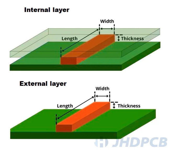
External and internal PCB trace width calculators differ mostly based on the position of the trace within the PCB.
External traces are those that are visible to the environment outside of the PCB, for instance, traces positioned on the board’s edge. The external trace width calculator pcb assesses additional factors that could impact the trace, such as humidity, airflow, and temperature. Since these factors can affect the trace’s ability to carry current and dissipate heat, the external trace width calculator may require different parameters than those used by the internal trace width calculator.
In contrast, internal traces are positioned within the PCB and, hence, are not visible to the environment. The internal trace width calculator presumes that the trace is surrounded by PCB material, which offers extra current-carrying capacity and dissipation of heat. As a result, the parameters employed in the internal trace width calculator could differ from those adopted by the external trace width calculator.
To summarize, the primary difference between external and internal PCB trace width calculators is the position of the trace and the additional variables that could impact its functionality. External traces frequently utilize microstrip lines, while internal traces usually use strip lines. Selecting the appropriate trace width calculator is crucial, and one should consider the trace’s location and the specific conditions it will face. Click for detailed guidance on microstrip and stripline in PCBs.
Calculation method of PCB internal and external wiring.
The calculation method for PCB trace width depends on whether it is an internal or external trace. For internal traces, the following formula can be used:
w = (I * K * T)/(ΔT * A)
where:
w = trace width (in mils)
I = maximum current (in amps)
K = thermal conductivity of copper (385 W/mK)
T = trace thickness (in oz/ft^2)
ΔT = maximum temperature rise (in Celsius)
A = cross-sectional area of the trace (in mils^2)
For external traces, the following formula can be used:
w = (I * K * T)/(ΔT * (0.048 * (T + 100)))
where:
w = trace width (in mils)
I = maximum current (in amps)
K = thermal conductivity of copper (385 W/mK)
T = trace thickness (in oz/ft^2)
ΔT = maximum temperature rise (in Celsius)
The calculation formula of PCB trace temperature.
The maximum temperature rise of a PCB trace can be calculated using the formula:
ΔT = (I^2 * R * t)/(K * A)
where:
ΔT = temperature rise (in Celsius)
I = current (in amps)
R = resistance (in ohms)
t = time (in seconds)
K = thermal conductivity of copper (385 W/mK)
A = cross-sectional area of the trace (in m^2)
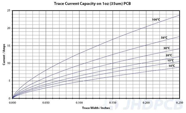
The calculation formula of PCB trace current.
The maximum current that a PCB trace can carry without overheating can be calculated using the formula:
I = (w * A * ΔT * 0.048)/(T + 100)
where:
I = current (in amps)
w = trace width (in mils)
A = cross-sectional area of the trace (in mils^2)
ΔT = maximum temperature rise (in Celsius)
T = ambient temperature (in Celsius)
The calculation formula of PCB trace resistance.
The resistance of a PCB trace can be calculated using the formula:
R = (ρ * L)/A
where:
R = resistance (in ohms)
ρ = resistivity of copper (1.68 x 10^-8 Ωm)
L = length of the trace (in meters)
A = cross-sectional area of the trace (in m^2)
The calculation formula of PCB trace voltage drop.
To calculate the voltage drop across a PCB trace, you can use a formula:
V = I * R
where:
V = voltage drop (in volts)
I = current (in amps)
R = resistance (in ohms)
The calculation formula of PCB trace power consumption.
To compute the power consumption of a PCB trace, you can use this formula:
P = I^2 * R
where:
P = power consumption (in watts)
I = current (in amps)
R = resistance (in ohms)