PCB Tear Drop

PCB Teardrops Roles and Rules in Designs

directory

What is PCB Teardrop?

PCB teardrops are essential features on a printed circuit board (PCB) that play a crucial role in the reliability and durability of electrical connections. A teardrop is a drop-shaped formation that appears at the junction between a trace and a via or pad on the PCB. This design modification is not just aesthetic; it serves important functional purposes.

During soldering, the interplay between the surface tension of the solder and that of the PCB substrate material results in the solder naturally forming a droplet-like shape at these connections. The teardrop shape, which can be either oval or circular, enhances the connection by strengthening the soldering joint. This design helps in reducing stress concentration, making the connection more robust and capable of withstanding mechanical and thermal stresses.

Moreover, the gradual widening of the copper trace as it approaches the hole or via ensures that the connection point is dependable. By preventing potential weaknesses in the connection, teardrops help to mitigate the risk of damage during the manufacturing process or due to environmental factors, thereby improving the overall reliability of the PCB.

What are the types of PCB teardrops?

As the core material of PCB, the three main raw materials for the production of CCL include glass fiber cloth, epoxy resin and copper foil, and PCB relies on them to realize the functions of conduction, insulation and support. Among them, glass fiber cloth and epoxy resin are often used as prepregs.

  1. Radial Teardrops
    Radial teardrops have a smooth, rounded contour that evenly extends around the perimeter of the pad. The trace connecting to the pad gradually widens into a tear-drop shape, providing a seamless transition. This design is particularly effective at enhancing stress relief and solderability. By creating a more gradual connection between the trace and the pad, radial teardrops distribute mechanical stress more evenly and improve the overall strength of the solder joint. However, this approach does consume additional board space around the pads, which might be a consideration in densely populated PCB layouts.
  2. Tangential Teardrops 
    Tangential teardrops present a different approach. In this design, the rounded contour is utilized solely on the side where the trace connects to the pad. The other edges of the pad stay straight, creating a more compact teardrop form. While tangential teardrops occupy less space compared to radial teardrops, they offer slightly less stress relief. This type is ideal for situations where space is constrained, and the trade-off between space efficiency and stress relief is acceptable.

Additional Techniques for Creating Teardrops

In addition to radial and tangential PCB design teardrops, there are other methods to achieve similar enhancements in PCB design:

different types of teardrops

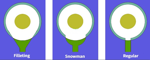
  • Filleting or Straight Technique
    Another common method is known as filleting or straightening, where multiple traces are added from the existing pad towards the trace. This approach creates a smooth transition that can enhance the connection’s mechanical strength and solderability, while being relatively simple to implement.
  • Snowman Technique
    The “snowman” method involves adding secondary pads at the junction where the existing pad meets the trace. These secondary pads are smaller and placed a few mils away from the center of the main pad. This technique provides a controlled way to improve stress distribution and solderability without significantly altering the overall PCB layout.

By understanding the differences between radial and tangential teardrops, as well as alternative techniques like the snowman method and filleting, PCB designers can make informed decisions based on their design goals, space constraints, and performance requirements.

What's the role of PCB teardrop?

the role of PCB teardrop

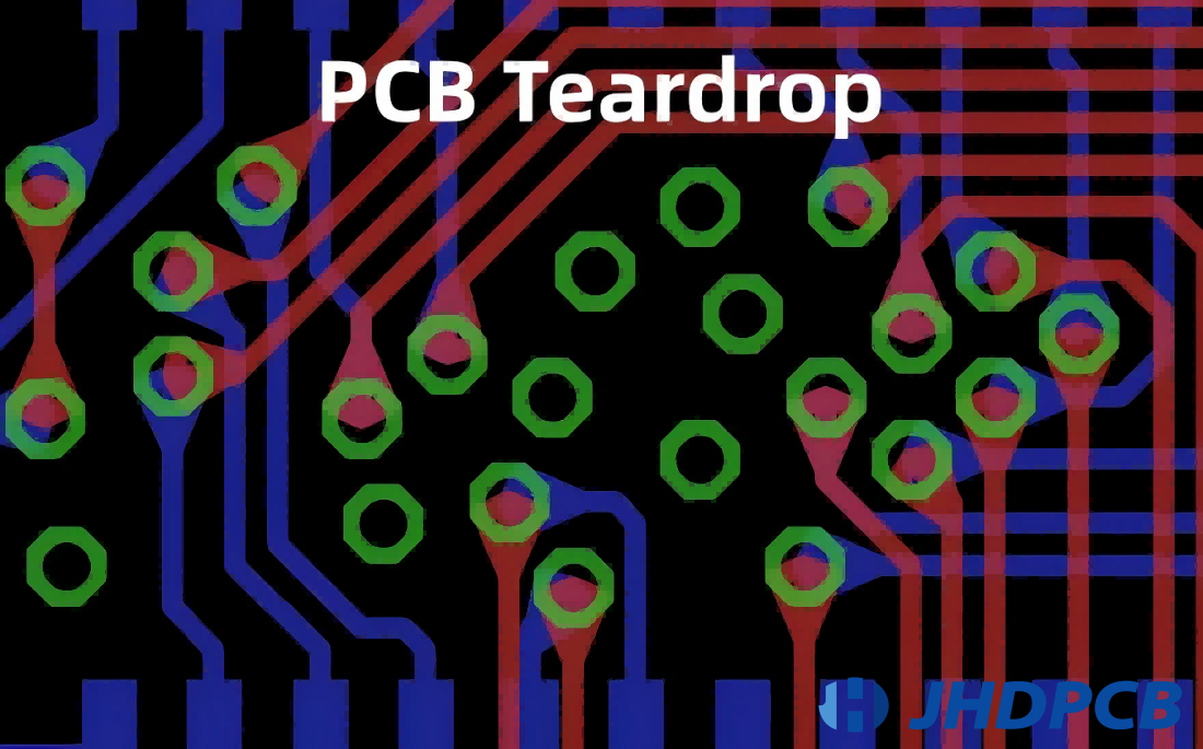
PCB teardrops are crucial design features in printed circuit boards (PCBs), offering several benefits that enhance the durability and performance of the board. Understanding their role can help designers and manufacturers achieve higher quality and reliability in their products. Here’s an in-depth explanation of why teardrops are significant:


PCB teardrops play a vital role in mitigating mechanical and thermal stress at the junctions between copper traces and pads or vias. When a trace connects to a hole or pad, stress concentrations can occur, especially where the copper trace transitions abruptly. This can lead to hairline cracks or breaks in the trace or the insulating substrate, particularly under mechanical stress or thermal cycling. The teardrop shape helps to distribute these stresses more evenly across a larger area, reducing the likelihood of such cracks. This is especially important in high-vibration environments or where there are frequent thermal changes, as it improves the board’s overall reliability.

During the soldering process, the quality of solder joints is crucial for a reliable electrical connection. Teardrop shapes increase the surface area for solder to adhere to, providing a better grip and ensuring a more robust solder joint. This additional surface area helps in achieving stronger, more reliable connections, which is particularly beneficial in high-density PCBs where space is limited and precision is critical.

PCB manufacturing involves precise drilling to create holes for vias and pads. However, slight deviations in drill bit positioning can occur, leading to potential misalignments. Teardrops act as a buffer zone that accommodates these minor deviations, ensuring that even if the drill bit is slightly off-target, the copper trace will still make a solid connection. This buffering effect helps to prevent ‘drill breakout,’ where the trace might otherwise become disconnected or poorly aligned due to slight inaccuracies during the drilling process.

In high-frequency signal applications, preserving signal integrity is crucial. Teardrop shapes assist in minimizing impedance fluctuations at connection points, which could otherwise cause signal degradation. By smoothing out transitions and connections, teardrops help ensure that signals travel through the PCB with minimal loss and interference. This reduction in impedance variations, known as PCB teardrop impedance, plays a crucial role in maintaining consistent performance and ensuring reliable signal transmission.

Teardrops enhance the overall reliability of the PCB by lowering the risk of open or weak connections. This not only helps to prevent electrical failures but also reduces the rate of board rejections during manufacturing.Fewer rejections mean lower production costs and improved cost-efficiency, making the teardrop design a valuable consideration in PCB manufacturing.

For specific applications like Ball Grid Arrays (BGAs), some designers use teardrops with no solder mask on the pads to increase the ball-to-land contact area, enhancing mechanical robustness. While this practice can be beneficial, it’s important to evaluate its necessity and potential impact on the overall design and manufacturing process.

Here’s a simplified table summarizing the improvements from using well-designed teardrops:

Improvement Area Benefit
Pad Lifting Defects Up to 75% decrease
Shorts and Leakage Current Issues 60% reduction
Solderability and Fillet Quality Up to 50% improvement
Opens and Connectivity Problems Around 40% reduction
Rework and Scrap Approximately 30% cost saving
Throughput and Production Efficiency 25% faster

In summary, teardrop in pcb are essential for improving the mechanical strength, soldering quality, and signal integrity of printed circuit boards. They tackle prevalent manufacturing issues and improve the overall functionality and dependability of electronic devices.

When and where to use PCB teardrops?

PCB teardrops are crucial in ensuring robust and reliable electronic designs, particularly when dealing with high-density or high-frequency circuits. Here’s a detailed guide on when and where to use teardrops in your PCB layout:

When to Add Teardrops

PCB teardrops are crucial in ensuring robust and reliable electronic designs, particularly when dealing with high-density or high-frequency circuits. Here’s a detailed guide on when and where to use teardrops in your PCB layout:

  • Final Stage of Design:
    It is highly recommended to incorporate teardrops at the final stage of your PCB design. This approach ensures consistency across different PCB manufacturers, as the teardrop creation process is often specific to each manufacturer’s capabilities. By involving your PCB layout engineer or designer, you can ensure that teardrops are added systematically and uniformly.
  • High-Frequency or RF Boards:
    For RF or high-frequency boards, precise control over PCB layout is essential. Teardrops should be integrated during the design phase to address any potential stress concentrations and ensure signal integrity.
  • Manufacturing Considerations:
    Many PCB fabricators have built-in teardrop creation engines that automatically add teardrops during the manufacturing process. Allowing the manufacturer to handle this can help maintain Design for Manufacturing (DFM) guidelines and keep your design’s integrity intact.
  • Software Capabilities:
    Some CAD systems offer an automated teardrop feature that can be enabled with a simple checkbox. In such cases, your PCB designer will handle the implementation, ensuring that teardrops are appropriately added based on the design rules set in the CAD software.

Where to Add Teardrops

  • Thru-Hole Drills:
    Teardrops are especially crucial near thru-hole drills where the ratio of trace to pad is minimal. They help distribute stress and prevent potential soldering issues or mechanical failures.
  • High-Density Boards:
    For dense boards, especially where vias are closely packed, adding teardrops helps maintain the integrity of the annular rings around vias, preventing issues during soldering and ensuring mechanical stability.
  • Flex-PCB Layouts:
    On flexible PCBs, teardrops reduce stress at the point where traces connect to pads, helping to mitigate issues caused by bending and flexing.
  • Under BGA (Ball Grid Array):
    When dealing with BGAs that include numerous vias, teardrops can alleviate stress and improve soldering quality by ensuring smooth transitions between traces and pads.
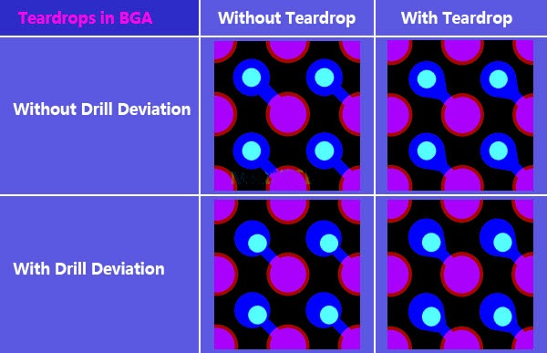
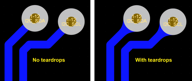
    BGA with Teardrops
  • Trace Exits:
    Incorporate teardrops where traces leave a pad, whether it’s a solid pad or one with a via. This helps prevent potential issues related to trace-to-pad transitions.
  • Narrow Traces:
    As traces become narrower, the need for teardrops increases. They help distribute stress more evenly and reduce the risk of trace damage or failure.
  • Large Conductors:
    For conductors larger than 20mil, teardrops are generally not necessary, as the larger size of the conductor can handle stress more effectively.

By adhering to these recommendations, you can improve both the reliability and ease of production of your PCB designs. Whether you choose to add teardrops manually or rely on your PCB manufacturer’s automated tools, ensuring that they are correctly implemented can significantly impact the performance and durability of your electronic products.

What are the PCB teardrop design rules?

When designing PCB teardrops, it’s essential to follow specific design rules to ensure the integrity and reliability of the circuit board. These rules help prevent issues like trace cracking, misalignment, and signal degradation. Proper use of teardrops in PCB design can greatly improve the mechanical durability and electrical performance of your board. Below is a detailed guide to these design rules:

  • Critical Junctions: Teardrops are primarily applied at all pad-to-trace and via-to-trace junctions. These junctions are particularly vulnerable during the manufacturing process, especially in the drilling and soldering stages. Applying teardrops at these points helps reinforce the connections, reducing the risk of trace cracking and improving the overall durability of the teardrop PCB.
  • Acute Angles: Traces that create sharp or narrow angles are prone to stress concentration. Applying teardrops at these locations smoothens the transition, ensuring better mechanical strength and reducing the likelihood of signal reflection or interference, which is crucial for high-speed circuits.
  • Large Copper Planes: For traces connecting to large copper planes or polygons, the sudden change in copper mass can lead to potential mechanical stresses or soldering issues. Teardrops facilitate a smoother transition from the trace to the plane, ensuring better structural integrity and more reliable solder joints.
  • Proportional Dimensions: The size of the teardrop should be carefully calculated based on the trace width to maintain a balance between mechanical reinforcement and spatial efficiency. The general guideline is to make the teardrop width approximately 1.2 times the trace width, and the radius about 0.6 times the trace width. These dimensions ensure that the teardrop is large enough to provide the necessary reinforcement but not so large that it interferes with adjacent traces or components.
  • Example Dimensions: For a trace width of 0.5mm, a typical teardrop would have a radius of 0.3mm and a width of 0.6mm. For narrower traces, such as 0.25mm wide, the teardrop would have a radius of 0.15mm and a width of 0.3mm. These specific dimensions are designed to optimize the PCB’s mechanical and electrical performance without compromising space.
Trace Width Teardrop Radius Teardrop Width
0.5mm 0.3mm 0.6mm
0.25mm 0.15mm 0.3mm
  • Curved Shapes:The teardrop should have a curved or rounded shape rather than a pointed one. A curved shape aids in solder flow during the assembly process, ensuring a more reliable connection. It also reduces the likelihood of stress concentration, which can lead to trace separation or cracking over time. This is especially crucial in high-density PCBs where the reliability of each trace is essential.
  • Avoiding Pointed Shapes: Pointed teardrops can create stress concentration at the tip, which can lead to failure during thermal cycling or mechanical stress. A smoothly rounded teardrop distributes stress more evenly, enhancing the durability of the connection.
  • Layer Consideration: In multi-layer PCB designs, it’s crucial to ensure that teardrops on one layer do not interfere with traces or vias on other layers. Careful planning is required to maintain layer alignment and avoid potential crosstalk or signal integrity issues. The teardrop implementation must be checked in the context of the entire PCB stack-up to prevent unintended design conflicts.
  • Automated Tools: Contemporary PCB design software frequently offers functions that enable designers to automate the placement of teardrops. These tools enable precise control over the teardrop size, shape, and placement, ensuring consistent application across the PCB. Designers can set specific parameters based on the trace width and desired teardrop dimensions, allowing the software to apply teardrops efficiently across the entire design.

By following these comprehensive design rules, PCB designers can effectively use teardrops to enhance the structural integrity of the PCB, improve signal reliability, and ensure a more robust final product. Proper implementation of teardrops is a critical step in preventing manufacturing defects and extending the lifespan of the circuit board.

Practical Applications of PCB Teardrops

PCB teardrops are essential for maintaining the reliability and functionality of electronic devices across multiple sectors. Here’s a closer look at how teardrops are used in different applications:

1. Consumer Electronics
In devices like smartphones and tablets, which feature densely packed PCBs, teardrops are essential for maintaining reliable connections between components. The compact design of these devices means that any failure in the connections can lead to significant issues such as dropped calls or malfunctioning touch screens. Teardrops help prevent such failures by reinforcing connections and reducing stress points, ensuring that the device performs reliably over time.

2. Medical Devices
Medical devices, including heart monitors, infusion pumps, and diagnostic equipment, require the highest level of reliability due to their critical role in patient care. Teardrops in the PCB designs of these devices contribute to their safety and effectiveness by ensuring robust and reliable connections. This helps in minimizing the risk of malfunctions, which is crucial for maintaining accurate monitoring and treatment functions.

3. Aerospace and Defense
In aerospace and defense applications, the dependability of electronic systems is paramount. Avionics and military equipment frequently function under harsh conditions and must operate without fail. Teardrops are vital for preserving the integrity of the connections in these systems, ensuring they stay functional in tough environments and enhancing the overall safety and effectiveness of aircraft and defense gear.

4. Automotive Electronics
Contemporary vehicles are fitted with a variety of electronic systems, ranging from engine control units to sophisticated infotainment systems. Given the harsh environments and demanding conditions within automotive applications, PCB teardrops help ensure the reliability and durability of these electronic systems. By providing additional reinforcement at critical junctions, teardrops help prevent failures that could affect vehicle performance and safety.

5. Industrial Equipment
In industrial settings, equipment often operates under demanding conditions, including high temperatures, vibrations, and exposure to various contaminants. PCBs in industrial machinery benefit from teardrops by gaining enhanced mechanical strength and reliability. This aids in reducing downtime and maintenance requirements, thereby enhancing the overall efficiency and longevity of industrial equipment.

6. Consumer Appliances
Everyday household appliances like washing machines, refrigerators, and microwave ovens use PCBs to control various functions. Teardrops in these PCBs ensure that the connections remain stable and reliable, reducing the likelihood of failures and ensuring the consistent operation of these appliances.

By incorporating teardrops in these practical applications, PCB designers can greatly improve the durability and performance of electronic devices, resulting in more reliable and efficient products across different industries.

Q&A with PCB teardrops

Teardrops in PCB refer to a specific design feature used to strengthen the connections between traces and pads. They are shaped like teardrops and help to improve the mechanical and electrical performance of the PCB by reducing stress concentrations at the junctions. This design technique can be particularly beneficial in high-speed and high-frequency applications.

Using teardrops to improve PCB quality helps by providing a smooth transition between the trace and the pad. This lowers the likelihood of mechanical stress and solder joint failure. Teardrops also enhance the electrical performance by minimizing impedance mismatches and reducing signal reflections, which is crucial for PCB teardrop high speed applications.

PCB teardrop accelerometer designs use teardrop shapes at the connection points between the accelerometer pads and the PCB traces to improve the mechanical and electrical performance. This design feature helps ensure stable and reliable connections, which is crucial for accurate sensor readings and the overall longevity of the accelerometer in the circuit. By reducing stress concentrations and minimizing impedance mismatches, teardrops enhance the reliability and precision of accelerometer applications in PCBs.

In conclusion, PCB teardrops are a vital design element that enhances the reliability and performance of electronic devices across various industries. By reinforcing critical connections and reducing the risk of manufacturing defects, teardrops play a key role in ensuring the longevity and efficiency of your products. Whether you are designing consumer electronics, medical devices, or aerospace systems, incorporating teardrops into your PCB layout can significantly improve the overall quality and reliability of your designs.

At JHDPCB, we understand the importance of precision in PCB design. With years of industry experience, we are dedicated to delivering top-quality PCB manufacturing services tailored to your precise specifications. If you have any questions or require support with your PCB design, our team of experts is ready to assist you. Contact us today to learn how we can support your next project.

Get a PCB Quote Now

Open high-quality PCB manufacturing services in JHDPCB

Leave a Comment