gold finger beveling

Gold Finger and Beveling in PCB

directory

What is Gold Finger?

Gold fingers are the gold-plated connectors located along the edges of a printed circuit board (PCB), designed to facilitate the connection between a secondary PCB and the motherboard of a device, such as a computer. These connectors are crucial for enabling communication between various digital devices, including smartphones and smartwatches. The reason gold is used for these connection points is its superior conductivity, which ensures efficient signal transmission. Gold fingers serve as a bridge, allowing signals to pass seamlessly between circuit boards, enabling commands to be processed swiftly and accurately across devices.

How to make Gold Finger PCB?

The production of Goldfinger PCBs requires a series of precise steps to guarantee the finished product complies with stringent requirements for electrical performance and longevity. Every stage is critical, from surface treatment to metal plating to quality inspection, all processes require a high degree of precision and expertise. The following outlines the specific stages involved in manufacturing a Goldfinger PCB.

The first step involves selectively covering the PCB surface, except for the areas where the gold fingers will be plated. Blue glue (a protective mask) is applied to shield the remaining portions of the board from the subsequent plating processes. This ensures that only the gold finger pads are exposed for treatment, while the conductive positioning is aligned with the direction of the PCB to ensure precision.

The copper pads, which will eventually become gold fingers, need to be free of oxidation to ensure strong adhesion during the plating process. To achieve this, the oxidation layer on the copper pads is removed using a sulfuric acid solution. After the acid treatment, the copper surface is thoroughly rinsed with water and then deionized water to ensure complete cleanliness. Following the rinse, a mechanical grinding process is applied to the surface of the copper pads to further enhance the removal of oxidation and improve the surface quality for plating. Another round of water and deionized water rinsing ensures that the copper is in its purest form, ready for the electroplating steps.

Once the copper pads are clean and prepared, the electroplating of a nickel layer begins. Nickel serves as the intermediary layer between the copper and the gold. Its purpose is to provide a durable, corrosion-resistant foundation for the gold, as well as improve the wear resistance of the gold fingers. Electroplating nickel requires carefully controlling the electric current, which deposits a uniform layer of nickel onto the copper surface. Once the nickel is electroplated, the pads are again cleaned using water and deionized water to ensure no residue remains from the electroplating process.

With the nickel layer in place, the next step is to electroplate the gold onto the nickel surface. This is where the PCB gets its “Gold Fingers” name. Hard gold is typically used due to its strength, wear resistance, and ability to withstand frequent insertions and removals in slots. Electroplating gold requires precise control of both the current and time to ensure the correct thickness (usually around 30μ”) of gold is deposited onto the nickel. Gold is selected due to its superior electrical conductivity and resistance to corrosion, particularly important in preventing PCB gold finger corrosion, making it perfect for durable and high-performance electrical connections. During this process, the leftover gold that does not adhere to the PCB is carefully collected and recycled to minimize waste, given that gold is a valuable material. After the electroplating process is finished, the gold-plated fingers are rinsed with water and deionized water to ensure the surface is clean and free of any impurities that might impact performance.

After the gold plating is complete, the protective blue glue that was applied in the first step is removed. This exposes the rest of the PCB, leaving the newly gold-plated fingers intact and ready for further processing. The board is now ready to proceed to the next phase of production, which typically involves solder mask printing.

The final step in making Gold Finger PCBs is a rigorous inspection process. Each PCB must undergo thorough quality control checks to ensure that the gold fingers meet the required standards for smoothness, pcb gold finger plating thickness, and adherence.

The inspection often includes visual checks under magnification to identify any surface defects, followed by adhesion tests to ensure that the gold plating is securely bonded to the underlying layers. If the plating lacks proper smoothness or fails the adhesion tests, the PCB cannot proceed to commercial release.

The whole process, while seemingly straightforward, requires precision at every stage to ensure that the gold fingers will function reliably, especially in environments where the PCB will undergo frequent insertion and removal. Only highly specialized PCB manufacturers with advanced equipment and expertise can perform the Gold Finger plating process to this level of detail and accuracy.

By following these meticulous steps, manufacturers can create PCBs with gold fingers that are not only highly conductive but also durable, making them suitable for a wide range of applications, from personal computers to industrial machinery.

What is gold finger beveling?

What is gold finger beveling?

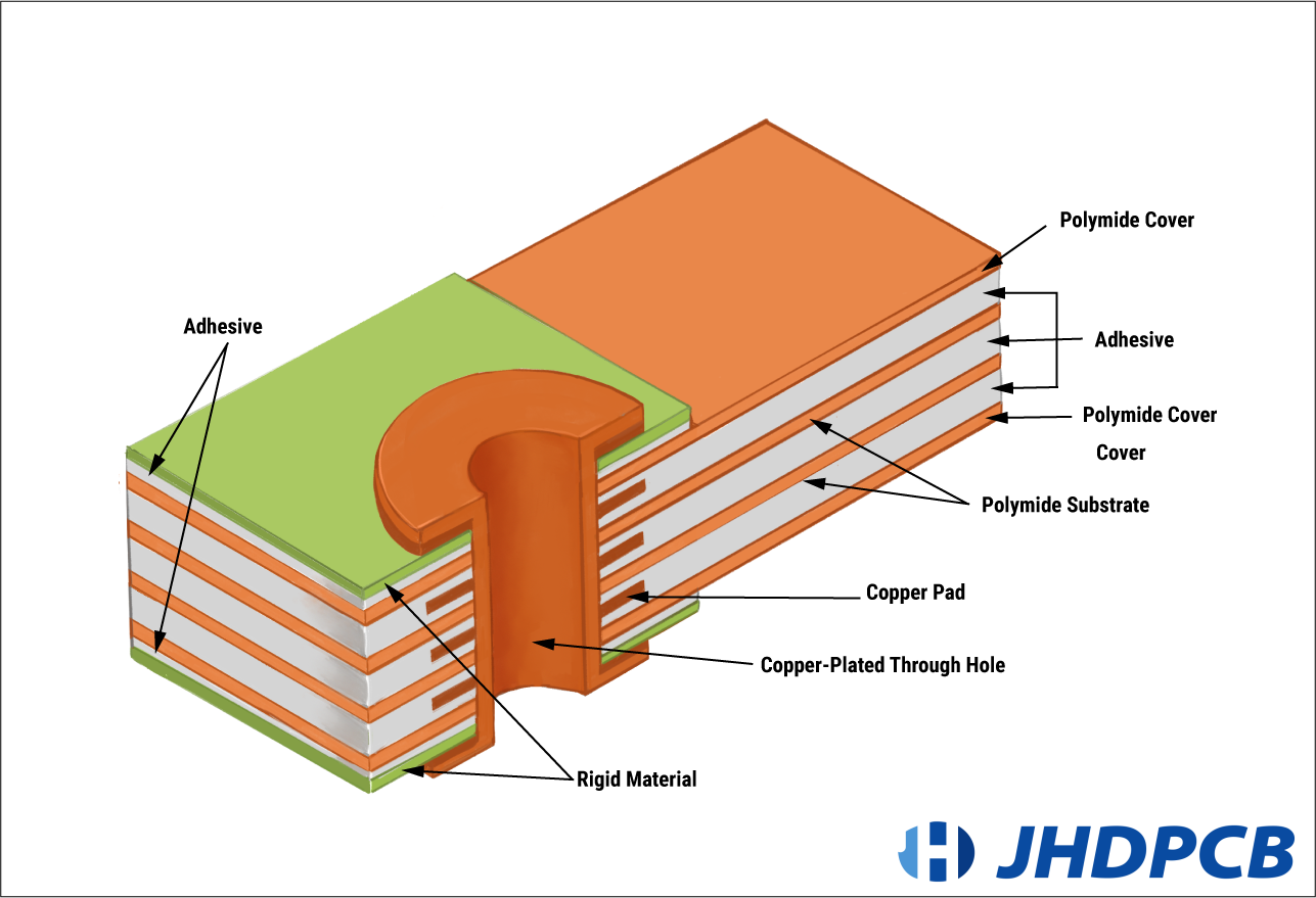
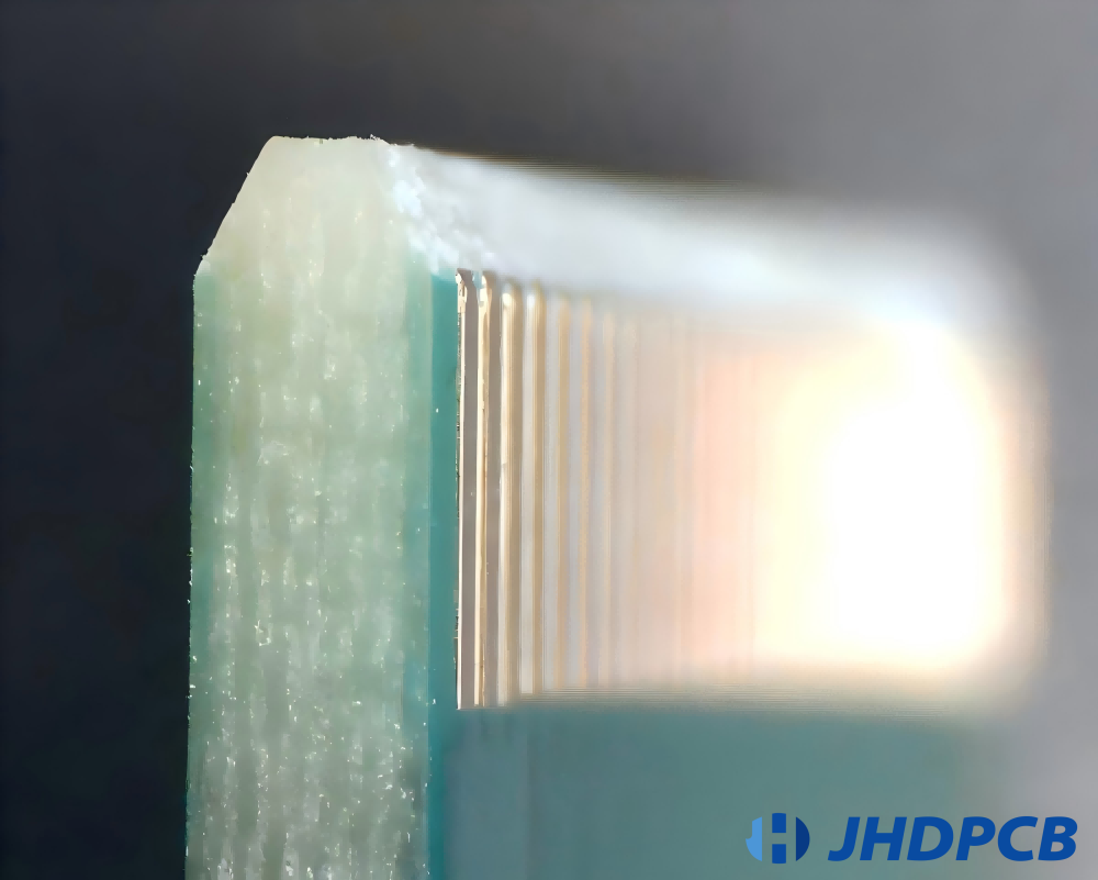
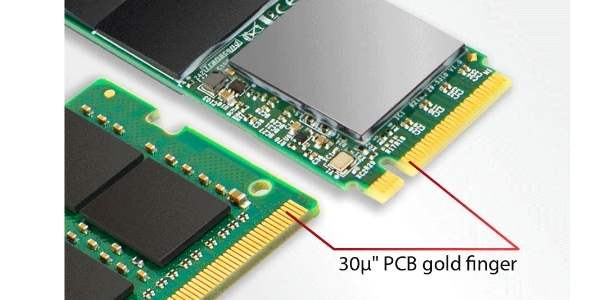
Gold finger beveling is an essential process in the manufacturing of printed circuit boards (PCBs) that involves creating a sloped edge at the PCB gold finger connector to ensure smooth insertion into corresponding slots. The process transforms the sharp, squared corners of the connector fingers into sloped or beveled edges, which not only enhances ease of insertion but also ensures durability and reliability in electronic connectors.

Purpose of PCB Gold Finger Beveling

The primary purpose of beveling the gold fingers is to facilitate easier and more precise insertion into the receiving slot of a connector, reducing wear and tear on both the PCB and the slot. Without beveling, the sharp edges would create resistance during insertion, increasing the likelihood of damaging the PCB or the slot over time.

Sometimes referred to as “beveled golden fingers,” these features are designed with slanted, rectangular shapes to further reduce mechanical stress during insertion and removal. The angled design allows for a gradual, smooth entry or exit from the socket, minimizing mechanical stress that could otherwise damage both the PCB and the slot. This gradual insertion mechanism is especially beneficial in prolonging the life of both components through repeated use.

Benefits Beyond Mechanical Performance

In addition to reducing physical stress, beveled gold fingers also offer significant improvements in optical and electrical performance. By providing a more stable and secure connection, the beveled edges enhance electrical contact between the gold fingers and the connector pins. This, in turn, improves signal transmission reliability, ensuring that electronic products function more consistently and without disruption. The sloped edges help align the gold fingers with the connector slot, ensuring that the connection is precise and stable, leading to improved overall performance.

Furthermore, the beveled edges make insertion easier and more fluid, requiring less force to properly connect the PCB to its respective slot, which in turn enhances the overall durability and lifespan of the electronic connectors.

The Beveling Process

Beveling is the final stage in the gold finger plating process, occurring after the solder mask is applied. This procedure is fully automated, utilizing specialized beveling machines to guarantee accuracy and uniformity. Here’s how the PCB gold finger plating process works:

  1. Nickel Plating:The connector edges of the PCB are initially plated with a layer of nickel, typically between 2 to 6 microns thick. Nickel serves as the base layer for the subsequent gold plating, ensuring a solid foundation for durability and electrical conductivity.
  2. Gold Plating:A hard gold layer, between 1 to 2 microns thick, is applied over the nickel. Manufacturers often alloy the gold with cobalt to improve surface resistance, which enhances the PCB’s ability to withstand frequent insertions and removals without wear or degradation.
  3. Beveling:After the plating process is completed, the edges of the gold fingers are beveled. The beveling angle typically ranges from 30° to 45°, depending on the port, the size of the circuit board, or specific client requirements. This tapering ensures easy insertion into the connector slot while reducing mechanical stress on both the PCB and the slot during use.
  4. Surface Finish Application: Once the beveling is finished, the next step involves applying the surface finish, ensuring a smooth, durable layer that further protects the gold fingers and improves the overall performance and longevity of the PCB in its final application.

The Importance of Angle Precision

Beveled Edge Angle (°) Application Requirements Performance Impact Example Devices/Industries
15° – 25° High insertion/extraction force, increased contact stability Increases contact area and friction, improving signal transmission stability Devices with frequent insertion/removal (e.g., connectors in telecom devices)
25° – 35° Balanced insertion/extraction requirements, moderate spatial constraints Provides a good balance between contact area and ease of insertion General-purpose electronics and industrial applications
35° – 45° Strict spatial constraints, compact designs Easier integration in tight spaces, slightly reduced contact area Miniaturized devices (e.g., smartphones, compact IoT devices)
  • Smaller angles (15° – 25°) are ideal for applications needing higher contact stability.
  • Larger angles (35° – 45°) are better suited for devices with tight spatial constraints, where ease of assembly is critical.
  • Precision in angle control, using advanced design tools and machining equipment, is essential to optimize PCB performance across various industries.

Gold Finger Layout Design Considerations

Plate Thickness (mm) Standard Beveled Edge Height (mm) CAM Copper Cutting (Single Side) (mm) Beveled Edge Height (When Finger is Far from Forming) (mm)
0.4 – 1.6 0.50 0.60 0.90 ± 0.10
2.0 0.65 0.75 1.05 ± 0.10

When designing the layout for PCBs with beveled edges, it’s essential to account for factors like the length, width, and position of the gold fingers. The bevel angle and depth must align perfectly with the length of the fingers. Improper alignment can lead to gold fingers that are either too short or too thin at the edges, rendering the PCB unusable. For instance, in PCBs with a thickness of 0.4-1.6mm, a standard beveled edge height is around 0.50mm, with copper cutting (CAM) on one side measuring about 0.60mm.

These parameters vary depending on the PCB thickness. For boards with a thickness of around 2.0mm, the beveled edge height increases to 0.65mm, and the copper cutting is about 0.75mm on one side. In production, it’s crucial to ensure that the bevel does not damage the gold fingers, as this would compromise the performance of the PCB.

Manufacturing Challenges and Costs

Designing beveled gold fingers is not without challenges. Achieving high precision during the manufacturing process requires advanced equipment and expertise. As a result, the processing cost is often higher than that of standard gold fingers. Manufacturers need to balance performance requirements with production feasibility and cost-effectiveness, especially when dealing with high-volume production runs.

Enhancing Performance and Durability

Beveled edge gold fingers are particularly advantageous in applications where PCBs are frequently inserted and removed. The beveled design reduces mechanical stress on the gold fingers during insertion and extraction, minimizing wear and improving overall reliability. This makes beveled gold fingers an ideal choice for devices requiring consistent and stable signal transmission, such as telecommunications equipment, medical devices, and high-performance computing systems.

As electronic devices become more compact and complex, the need for reliable and efficient PCB designs grows. The PCB beveled edge process, particularly for gold fingers, offers significant improvements in durability, signal transmission stability, and ease of assembly. For engineers and designers working on cutting-edge electronics, considering beveled edges in PCB design is a practical solution that ensures long-term performance and reliability. Despite the added manufacturing challenges and costs, the benefits of beveled gold fingers make them an essential technology in the evolution of modern electronics.

What different from Gold Fingers and PCB Edge Connectors?

Illustration of an Edge Connector displayed in a CAM system

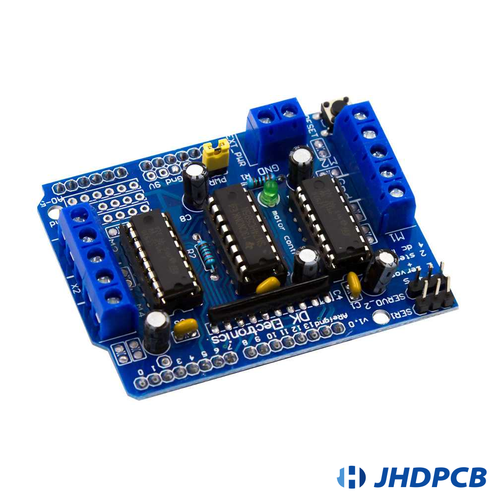
In the world of printed circuit boards (PCBs), both gold fingers and edge connectors play vital roles in ensuring effective communication between different components or external devices. Despite their similarities in functionality, these two elements are distinct in several ways. Understanding the differences between gold fingers and edge connectors is crucial for proper PCB design, as each serves specific purposes and comes with its own set of design, usage, and cost considerations.

One of the most significant differences between gold fingers and edge connectors lies in their usage.

Gold Fingers: These are primarily designed to connect a PCB to peripheral devices or other circuit boards, enabling communication or data transfer. Gold fingers create an interface that allows for frequent insertion and removal, making them ideal for components like USB devices, expansion cards (such as PCIe, PCI, or AGP cards), or storage cards like SD cards. This flexibility in plugging and unplugging makes gold fingers a preferred choice when repeatable, reliable connections are needed without significant wear and tear on the board or device.

Edge Connectors: On the other hand, edge connectors are fixed slots or sockets used for more permanent connections. They are typically used to interface expansion cards or modules directly with the motherboard in computers, as seen in PCIe slots. Unlike gold fingers, edge connectors are generally not meant for frequent plugging and unplugging once installed, and their primary purpose is to establish a stable, long-term connection between the PCB and the rest of the system.

Another key distinction between gold fingers and edge connectors is their placement on the circuit board.

Gold Fingers: As the name implies, gold fingers are positioned along the edge of the PCB. This positioning allows them to slide directly into a slot or connector, creating a seamless interface with external devices or peripheral components. Their specific placement on the edge is critical for enabling the smooth insertion and removal of connected components.

Edge Connectors: Unlike gold fingers, edge connectors do not have a predefined location and can be placed anywhere on the PCB as needed. Their location is typically determined by the overall design and layout of the board. Edge connectors are designed as permanent fixtures that stay in place, unlike the more flexible nature of gold fingers.

The construction and design of gold fingers and edge connectors differ significantly, mainly due to their distinct applications.

Gold Fingers: Gold fingers are formed as metal contacts along the edge of a PCB. They are coated with a thin layer of hard gold (typically mixed with cobalt) to enhance conductivity and withstand wear from frequent use. The gold plating process requires precise milling of the edges, ensuring that the beveling is done correctly (typically at angles between 30 and 45 degrees) for smooth insertion into corresponding slots. The pcb gold finger plating enhances both electrical conductivity and durability, allowing for thousands of connection cycles without significant degradation.

Edge Connectors: In contrast, edge connectors are more akin to sockets or receptacles. These connectors are often enclosed in a thermoplastic casing, with one side open to allow the connection of pins or contact points. Inside the edge connector, rows of metallic contacts are used to interface with a compatible component, such as a PCIe card. Unlike gold fingers, edge connectors do not require gold plating, making them less expensive to manufacture. They are typically made from a combination of plastic and metal, and the contacts are inserted into through-holes on the board and soldered in place.

Due to their different roles and designs, gold fingers and edge connectors exhibit varying levels of durability and conductivity.

Gold Fingers: The use of gold plating in the manufacturing of gold fingers significantly enhances their conductivity and resistance to wear. Gold, being an excellent conductor, ensures low electrical resistance and stable data transmission over time. Moreover, the hardness provided by the cobalt alloy enhances the physical durability of the contact points, minimizing PCB gold finger damage and allowing for frequent use without wear.

This makes gold fingers ideal for applications requiring repeated connections and disconnections, such as in consumer electronics and computer peripherals.

Edge Connectors: While edge connectors are not typically plated with gold, they still provide reliable electrical connections, albeit at a lower cost. The materials used in edge connectors, such as copper or other conductive metals, are sufficient for permanent or semi-permanent connections where frequent disconnection is not a concern. However, since they lack the wear resistance and conductivity of gold-plated contacts, edge connectors are less suited to environments where high durability and repeated connections are needed.

Cost is another critical factor that differentiates gold fingers from edge connectors.

Gold Fingers: Due to the use of gold plating, gold fingers are more expensive to manufacture. Gold is a costly material, and the process of plating the fingers with a thin layer of hard gold increases production costs. Additionally, the precise milling required to bevel the edges of the gold fingers adds complexity and labor to the manufacturing process. However, the higher cost is justified by the superior conductivity, durability, and performance in applications that demand frequent and reliable connections.

Edge Connectors: In contrast, edge connectors are relatively inexpensive to produce. Since they do not require gold plating or complex manufacturing steps like beveling, they are cheaper to make. Edge connectors are typically fabricated from plastic and metal components, which are less expensive than gold. This makes them an affordable choice for applications where durability and conductivity requirements are lower, and permanent or semi-permanent connections are sufficient.

While gold fingers and edge connectors both serve as connection points on a PCB, they are fundamentally different in design, functionality, placement, durability, and cost. Gold fingers excel in scenarios that require frequent, reliable connections with high conductivity and durability, making them ideal for consumer electronics and expansion cards. Edge connectors, on the other hand, are designed for more permanent connections and are a cost-effective solution in situations where repeated plugging and unplugging are unnecessary.

Understanding these distinctions is crucial for engineers and designers when deciding which type of connector to use in their PCB designs, ensuring optimal performance and cost-efficiency for the intended application.

Aspect Gold Fingers Edge Connectors
Functionality Connects the PCB to peripheral devices or other circuit boards. Allows frequent connections and disconnections. Used for more permanent connections, typically expansion slots like PCIe or PCI.
Placement Located specifically on the edge of the PCB. Can be placed anywhere on the PCB based on design requirements.
Design Gold-plated solder pads, usually beveled at 30-45 degrees for easy insertion. Enclosed in a thermoplastic casing, with pins inserted into through-holes.
Conductivity High conductivity due to gold plating. Moderate conductivity, usually made from copper or other metals.
Durability Durable and wear-resistant due to gold plating, suitable for repeated use. Less wear-resistant, designed for permanent or semi-permanent use.
Cost Expensive to manufacture due to the gold plating process. Cheaper to produce, made from plastic and metal materials.
Usage Ideal for applications requiring frequent connection/disconnection, such as USB, SD cards, and expansion cards. Suitable for permanent connections like PCIe, PCI, or AGP slots.

How to clean Gold Finger PCB?

Gold fingers on PCBs (Printed Circuit Boards) are essential for providing dependable electrical connections between components. However, over time, gold fingers can accumulate dirt, oils, oxidation, and other contaminants, which can degrade performance. In this guide, we’ll walk you through the essential steps to properly clean gold finger PCBs and ensure optimal performance.

Why Cleaning Gold Finger PCBs Is Important

Contamination on gold fingers can lead to a range of issues, including:

  • Increased Contact Resistance: Dirt and grime can increase electrical resistance, leading to intermittent connections or complete failure.
  • Signal Integrity Degradation: Dirty contacts may impair the transmission of signals, which can result in data errors.
  • Wear and Tear: Inserting dirty gold fingers into slots or connectors accelerates wear, which shortens the lifespan of both the PCB and the mating connector.

To prevent these problems, regular cleaning of gold finger PCBs is essential. Let’s explore how to do it effectively.

Damaged gold finger PCB

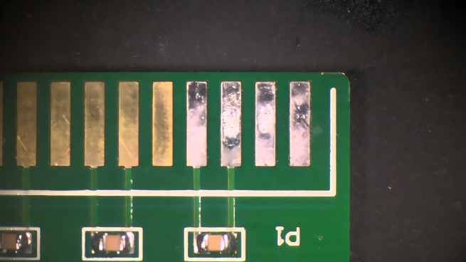
Before beginning the cleaning process, conduct a visual inspection of the gold fingers to evaluate their state. Here’s what to check for:

  • Discoloration: This may indicate oxidation or the presence of contaminants.
  • Scratches or Abrasions: Any physical damage that could impair the function of the connectors.
  • Accumulated Debris:Dust, oil, or any visible grime should be noted before cleaning.

Use a magnifying glass or microscope for a detailed inspection, especially if the board has been in heavy use. Focus on the chamfered edges of the fingers, as these regions typically endure the most wear.

Once the inspection is complete, it’s time to remove surface contaminants such as oils, dust, and particulate matter. For this, follow these steps:

  • Use High-Purity Isopropyl Alcohol (IPA): The preferred cleaning solvent for gold finger PCBs is 99% pure isopropyl alcohol. Avoid lower concentrations, as they contain water and could leave residue behind. Dampen a lint-free swab or cloth with IPA.
  • Gently Wipe the Gold Fingers: Lightly rub the swab along the length of each gold finger. Move in one direction, rather than scrubbing back and forth, to avoid friction that could damage the plating. Use a soft touch to prevent any scratches on the gold surface
  • Repeat if Necessary: For heavily contaminated areas, you may need to do multiple passes with fresh IPA and clean swabs.
  • Blow Away Loose Particles: After wiping, utilize compressed air or an air duster to eliminate any leftover dust or fibers. This step guarantees that the surface is entirely clean and devoid of debris.

Gold is highly resistant to corrosion, but over time, even small amounts of oxidation can form on the surface. Oxidized areas appear dull and darker than the rest of the gold plating. To restore the original shine and conductivity, follow these techniques:

  • Use a Pencil Eraser: A simple pencil eraser is often effective for removing light oxidation. Gently glide the eraser across the affected regions in one direction to prevent harming the plating.
  • Fiberglass Scratch Brushes: For more severe oxidation, consider using a fiberglass scratch brush. These are specially designed for PCB cleaning and provide enough abrasion to remove oxidation without harming the gold surface. Light pressure is key—over-scrubbing could remove the thin gold layer, exposing the copper underneath.
  • Swab Again with IPA: After removing oxidation, clean the surface with IPA to remove any eraser residue or particles dislodged during the cleaning process.

Sometimes, you may encounter stubborn contaminants like hardened grime, flux residues, or adhesives. These require more robust cleaning techniques:

  • Heated IPA Soak: Soaking the gold fingers in heated isopropyl alcohol can help loosen hardened grime. After soaking for a few minutes, use a nylon brush to gently scrub the fingers and then wipe them down with a fresh IPA swab.
  • Ultrasonic Cleaning: For more sophisticated cleaning, ultrasonic cleaners can be utilized. These devices employ high-frequency sound waves to generate tiny bubbles that help remove contaminants.Combine this with a mild cleaning solution for best results, and always rinse with IPA afterward.
  • Chemical Cleaners for Flux: If flux or solder splatter is present, use a dedicated flux remover. Be sure to select a product safe for use on gold-plated surfaces. Always follow up with IPA to remove any residue left behind by the cleaning agent.

Once the gold fingers have been cleaned and any oxidation or contamination removed, ensure the connectors are thoroughly dry before reinsertion into any slots or connectors:

  • Compressed Air: Use compressed air to quickly dry the gold fingers and remove any leftover solvent.
  • Allow Time for Evaporation: If you don’t have access to compressed air, allow the PCB to sit in a clean, dust-free environment for a few minutes until all the IPA has evaporated completely.

Best Practices for Cleaning Gold Finger PCBs

Adhering to these recommended practices will contribute to efficient and safe cleaning:

  • Use Lint-Free Materials: Always use lint-free swabs and cloths to prevent fibers from sticking to the gold fingers.
  • Avoid Excessive Force: Whether using an eraser, brush, or swab, light pressure is key. Gold plating is very thin, and excessive force can wear it down.
  • Work in a Clean Environment: Dust and airborne particulates are a constant threat during cleaning. Operate in a tidy, static-free setting to reduce contamination throughout and following the process.
  • Regular Maintenance: Periodically clean the connectors and mating slots to maintain optimal contact and prolong the life of both the PCB and its connectors.

Maintaining clean gold finger PCBs is crucial for preserving signal integrity, reducing wear, and ensuring long-term reliability. By following the outlined steps—visual inspection, cleaning contaminants, removing oxidation, and dealing with heavy buildup—you can ensure that your PCBs operate at their peak performance.Integrating these cleaning procedures into routine maintenance schedules will assist in preventing downtime and avoiding expensive PCB gold finger repairs or replacements.

Q&A for Gold Finger

The main difference between gold bonding finger PCB and golden finger PCB lies in their applications and design. Gold finger PCB features conductive strips on the edges, typically used for connecting circuit boards to other devices, such as in memory modules. In contrast, gold bonding finger PCB is specifically designed for semiconductor chip packaging, allowing for stable connections between the chip and the PCB through bonding processes. While both utilize gold-plated connections for enhanced conductivity and durability, gold finger PCBs focus on ease of insertion and connection, whereas gold bonding finger PCBs are tailored for efficient signal transfer in integrated circuits.

Plated through holes are essential in PCB design as they provide electrical connectivity between different layers of the board. They work in conjunction with gold fingers and edge connectors to create reliable connections, ensuring that signals are transmitted effectively throughout the device.

The manufacturing process for PCB gold fingers typically includes the plating of through holes, surface finish application, and solder mask preparation. Gold plating is applied to the edges of the PCB to enhance conductivity and protect against oxidation.

Gold-plated connectors on PCBs ensure low-resistance electrical connections, which are crucial for the efficient operation of peripheral devices. They help in maintaining signal integrity, especially in high-speed applications like graphics cards.

Gold-plated connectors on PCBs ensure low-resistance electrical connections, which are crucial for the efficient operation of peripheral devices. They help in maintaining signal integrity, especially in high-speed applications like graphics cards.

Devices that commonly utilize PCBs with gold fingers include sound cards, graphics cards, and various other peripheral devices. These gold-plated connectors are vital for ensuring proper electrical communication and signal transmission between components.

In summary, PCB gold fingers play a vital role in ensuring reliable connections between the PCB and other components, especially in high-performance applications. Proper design, manufacturing, and maintenance of these connectors are essential for optimal performance, durability, and longevity. From beveling to ensure smooth insertion to regular cleaning for maintaining signal integrity, every step in the handling of PCB gold fingers contributes to the overall success of the electronic system.

At JHDPCB, we pride ourselves on delivering high-quality PCB solutions with precision engineering. Our expertise in gold finger beveling ensures reliable connections and long-lasting performance. Leveraging cutting-edge technology and a dedication to quality, JHDPCB is your reliable partner for all your PCB requirements.

Get a PCB Quote Now

Open high-quality PCB manufacturing services in JHDPCB

Leave a Comment