The main difference between Copper thieving and Copper balancing lies in their purpose and application within Printed Circuit Board (PCB) design:
1.Clearance:
Copper thieving must maintain sufficient clearance from signal traces to prevent interference.
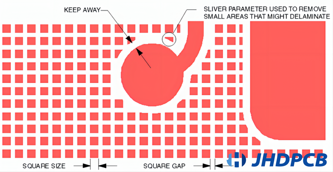
- Ensure a minimum distance between thieving features and adjacent signal traces, typically three times the trace width.
- Utilize design rule checks (DRCs) in PCB design software to enforce clearance requirements.
- Employ guard traces or keep-out areas to maintain separation between thieving and signal traces.
2.Net Assignment:
Copper thieving should be connected to a designated net, usually ground, to avoid floating copper.
- Directly connect thieving features to the ground plane or ground net using vias or traces.
Use net tie components to ensure a solid electrical connection between thieving and the designated net.
3.Transmission Mode Alteration:
Thieving patterns can influence transmission modes, potentially affecting signal integrity.
- Employ simulation tools to analyze the impact of thieving on transmission line characteristics.
- Adjust thieving patterns to minimize impedance variations and maintain consistent transmission performance.
- Consider tapered or meandered thieving patterns to mitigate impedance disruptions.
4.Signal Integrity:
Thieving should not compromise signal integrity or introduce signal distortions.
Avoid placing thieving features near high-speed signal paths or critical signal traces.
- Perform signal integrity simulations to assess the impact of thieving on signal quality and make adjustments accordingly.
- Utilize controlled impedance routing techniques to maintain signal integrity in thieved areas.
5.Solderability:
Thieving patterns should not hinder soldering processes or affect solder joint quality.
- Ensure thieving features do not overlap with solder pads or component mounting areas.
- Select solder mask materials compatible with thieving patterns to prevent solder bridging or adhesion issues.
Conduct solderability testing to verify the compatibility of thieving designs with assembly processes.
6.Structural Integrity:
Thieving should not compromise the mechanical stability or strength of the PCB.
- Distribute thieving features evenly across the copper thieving pcb to prevent localized stress concentrations.
- Avoid placing thieving patterns in areas prone to mechanical stress, such as near mounting holes or board edges.
Perform mechanical stress analysis to ensure thieving does not compromise board reliability.
7.Electrical Isolation:
Thieving patterns must remain electrically isolated from active circuits to prevent unintended conductive paths and minimize the risk of accidents such as copper thieves electrocuted.
- Implement physical barriers, such as solder mask, between thieving features and active circuitry, to create a protective barrier against inadvertent contact.
- Conduct continuity tests to verify the absence of unintended electrical connections between thieving and signal traces, ensuring the safety of both personnel and equipment.
- Utilize clearance rules and isolation guidelines during PCB layout to maintain electrical separation, reducing the likelihood of hazardous situations such as copper thieves being exposed to live electrical currents.
8.Strategic Placement:
Thieving patterns should be strategically placed to optimize copper distribution and address areas with uneven copper coverage.
- Identify regions with limited copper exposure or high-component density for targeted thieving implementation.
- Concentrate thieving features in areas requiring additional copper balancing while avoiding interference with critical components or signal paths.
- Use copper distribution analysis tools to identify optimal locations for thieving patterns based on specific design requirements.
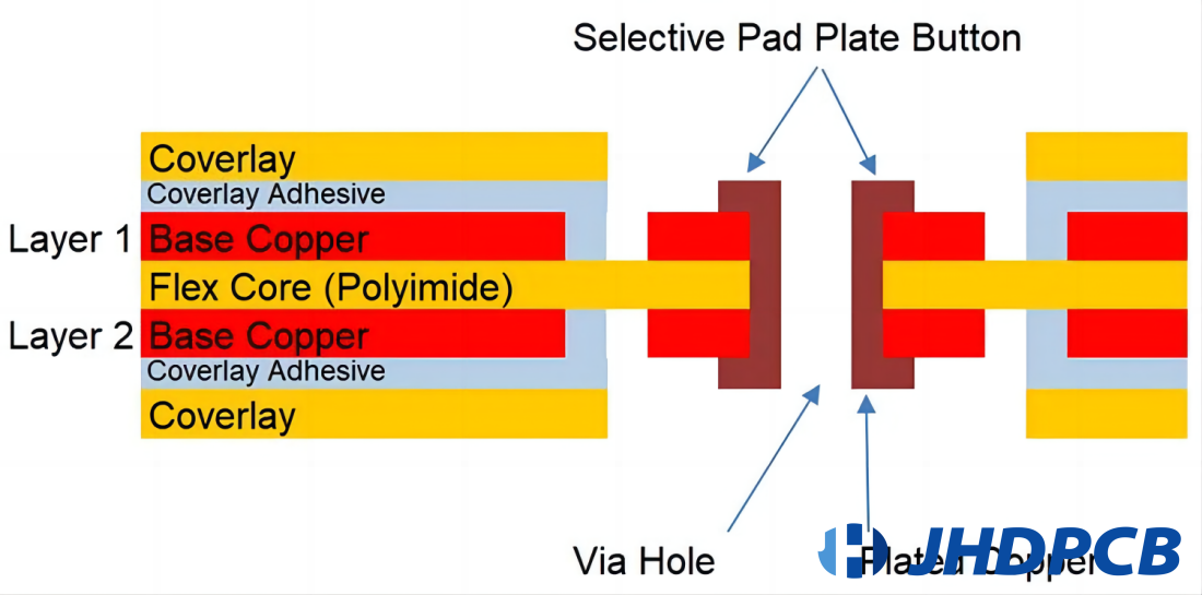
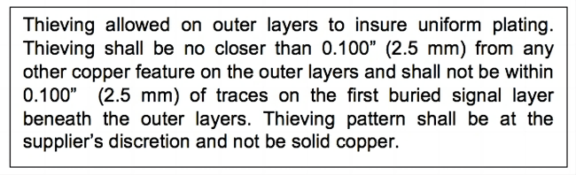
Should there be traces on the layers directly beneath where thieving is implemented, the impedance of these traces could be negatively impacted by the presence of thieving. To prevent this occurrence, it is imperative to include a note on the fabrication drawing specifying whether thieving is permissible and its designated locations. The following is one way to specify this on a fabrication drawing:
By carefully considering these factors, designers can effectively implement copper thieving into their PCB layouts without compromising the performance or reliability of their designs.
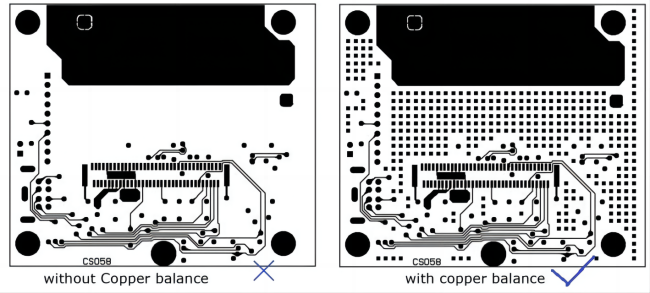
The primary function of copper thieving in printed circuit board (PCB) design is to achieve a more uniform distribution of copper across the PCB layers. This serves several purposes:
- Uniform Copper Distribution:
Copper thieving involves adding small copper features or patterns in areas where there is excess copper or where copper density needs to be balanced.This contributes to attaining a homogeneous copper distribution throughout the layers of the PCB.Without thieving, certain areas may have too much copper, leading to over-etching during the manufacturing process. - Control of Etching and Plating:
During PCB manufacturing, copper is typically etched away to create traces and patterns. Thieving helps maintain a consistent copper density, ensuring that the etching process removes the right amount of copper and doesn’t leave behind excess or insufficient copper on the board. This also applies to plating processes where copper is added back to the board. - Maintaining a uniform final thickness:
Thieving aids in ensuring a consistent final thickness of the PCB. Uneven copper distribution can result in variations in the final thickness of the board, which may affect its mechanical properties and compatibility with assembly processes. Thieving helps balance copper density to avoid these issues. - Minimizing Warping and Twisting:
PCBs can warp or twist during manufacturing or when exposed to heat if there are uneven copper distributions. Thieving helps minimize these issues by ensuring that copper is distributed evenly across the board, leading to a more stable and reliable PCB.
- Regulation of Dielectric Thickness:
Thieving additionally assists in managing the thickness of the dielectric substrate between copper layers. By managing copper distribution, designers can ensure the correct amount of dielectric material is used, preventing problems like electrical crosstalk between adjacent traces. - Cost Reduction:
Optimal copper distribution through thieving reduces material waste during manufacturing processes such as chemical etching. This effectiveness not only reduces manufacturing expenses but also promotes a greener and more eco-friendly production method.
In summary, copper thieving is essential for achieving uniformity, controlling dimensional stability, ensuring electrical performance, and optimizing production costs in PCB design and manufacturing.
1.Preparation:
Before initiating the copper thieving process, the PCB undergoes a preparatory phase where it is thoroughly cleaned. This cleaning step is crucial for removing any contaminants or residues that might interfere with subsequent plating operations. Contaminants on the PCB surface can lead to poor adhesion of plating materials or cause defects in the final product. Consequently, it is imperative to guarantee that the PCB is free of contaminants prior to advancement in order to attain superior outcomes.
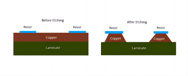
2.Application of Resist:
The subsequent stage entails administering a resist substance onto the PCB surface. This resist substance serves as a safeguarding stratum, safeguarding specific regions of the PCB from the ensuing copper plating procedure. Ordinarily, the employed resist substance is photosensitive, indicating that it undergoes a chemical alteration upon exposure to light. This characteristic facilitates accurate formation of the resist coating through photolithography methodologies. By applying the resist, specific areas of the PCB are designated for copper thieving, while others remain protected.
3.Exposure and Development:
Once the resist material is applied to the PCB, it undergoes exposure to light through a photomask. The photomask contains a pattern that defines the areas where copper thieving is required. Upon exposure to light, the resist substance undergoes a chemical response, resulting in either solidification or softening, contingent upon the variety of resist utilized. After exposure, the PCB is developed using appropriate chemicals to remove the unexposed resist, revealing the desired pattern for copper thieving. This step is critical for accurately defining the thieving areas on the PCB surface.
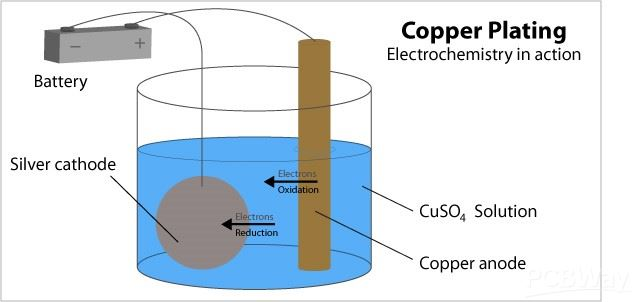
4.Copper Plating:
With the resist pattern in place, the PCB undergoes the copper plating process. During plating, the PCB is immersed in a plating solution containing dissolved copper ions. An electrical charge is administered to the PCB, prompting copper ions to migrate and adhere to the uncovered sections of the PCB exterior. Since the resist prevents copper deposition in protected areas, only the designated thieving areas receive additional copper plating. Consequently, it leads to a more consistent dispersal of copper throughout the PCB, aiding in alleviating concerns such as irregular plating and excessive etching.
5.Etching:
Following copper plating, the resist material is removed from the PCB surface, exposing the entire board. The PCB then undergoes an etching process to selectively remove excess copper from areas not designated for thieving. Etching involves immersing the PCB in an etchant solution that dissolves copper but does not affect other materials such as the substrate or solder mask. Through this process, the final copper traces and features on the PCB are defined, ensuring they meet the desired specifications for conductivity and connectivity.
6.Final Inspection:
Once the copper thieving process is complete, the PCB undergoes a thorough inspection to verify the quality of the finished product. Inspection may involve visual examination, electrical testing, or other quality control measures to ensure that the copper distribution is uniform and meets the required standards. Any deviations or defects identified during inspection can be addressed before the PCB is used in electronic assemblies, ensuring the overall reliability and performance of the final product.
- Uniform Electroplating: Copper thieving ensures even distribution of electroplating current, preventing issues like excessive copper in some areas and inadequate copper in others, leading to improved PCB quality and reliability.
- Enhanced Solderability: By providing a stable copper foundation, copper thieving helps in creating strong and durable solder joints, crucial for the overall performance and longevity of the PCB.
- Maintaining Signal Integrity: Copper thieving aids in preserving the transmission line impedance, especially important for high-speed digital signals and RF circuits, thus reducing signal loss and ensuring data accuracy.
- Improved Thermal Management: When properly implemented, copper thieving can help in more efficient heat dissipation from the PCB, which is crucial for maintaining component reliability and longevity.
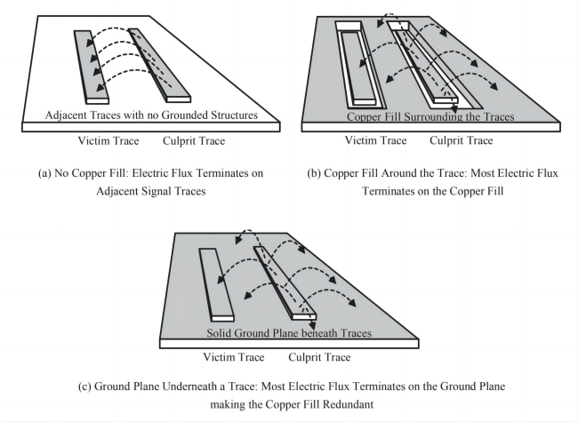
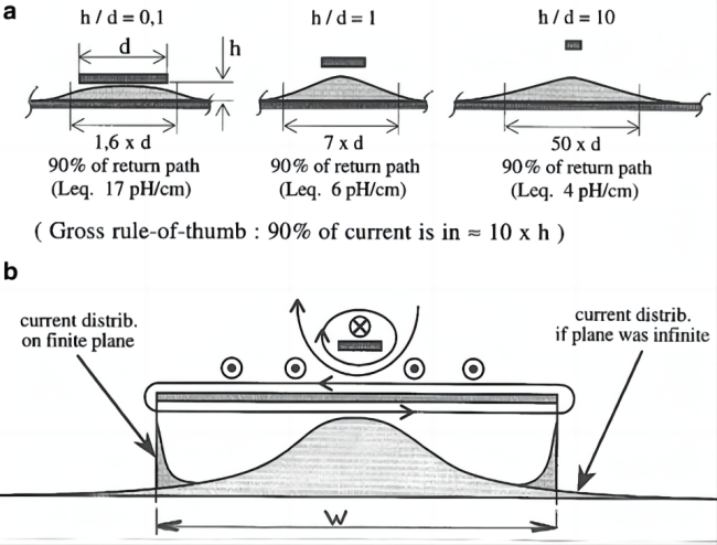
- Reduced Electromagnetic Interference (EMI): Copper thieving can aid in reducing electromagnetic interference between components and traces on the PCB, resulting in better overall electromagnetic compatibility (EMC) performance.Essentially, they function as patch antennas, helping to maintain signal integrity and reduce electromagnetic interference. See image below for illustration.
- Enhanced Manufacturing Yield: By promoting more uniform electroplating and solderability, copper thieving can lead to fewer defects during manufacturing, thereby increasing the overall yield of PCB production.
The ramifications of omitting thieving on the outer layers of PCBs with irregular distributions of features to be plated can be substantial:
- Uneven Copper Plating: In the absence of thieving, characteristics that are isolated or exhibit reduced copper coverage may fail to undergo proper plating, leading to non-uniform distribution of copper across the surface of the PCB. This can lead to variations in trace impedance and finished hole sizes, affecting the overall performance and reliability of the PCB.
- Excessive Copper Build-Up: Features that are densely packed or have a higher demand for copper may receive excessive plating, causing issues such as reduced finished hole sizes or compromised trace integrity. This can lead to manufacturing defects and may require additional corrective measures to rectify.
- Dimensional Inaccuracies: The lack of thieving can result in variations in the dimensions of plated features, such as holes for press-fit connectors. Without uniform copper plating, it becomes challenging to meet dimensional tolerances, potentially leading to assembly issues or component compatibility problems.
- Impact on Manufacturing Costs: Correcting non-uniform copper plating issues after fabrication can be time-consuming and costly. It may involve additional processes such as rework or scrapping of defective PCBs, leading to production delays and increased expenses.
- Diminished Dependability: Irregular copper plating has the potential to undermine the reliability and functionality of the PCB, particularly in pivotal scenarios demanding precise electrical attributes. This can result in increased failure rates and warranty claims, negatively impacting the reputation of the manufacturer.
Overall, the consequences of not incorporating thieving in outer layer PCB designs can affect various aspects of manufacturing, performance, and reliability, highlighting the importance of proper copper plating techniques in PCB fabrication processes.