Gold finger
directory
What is a Gold Finger?
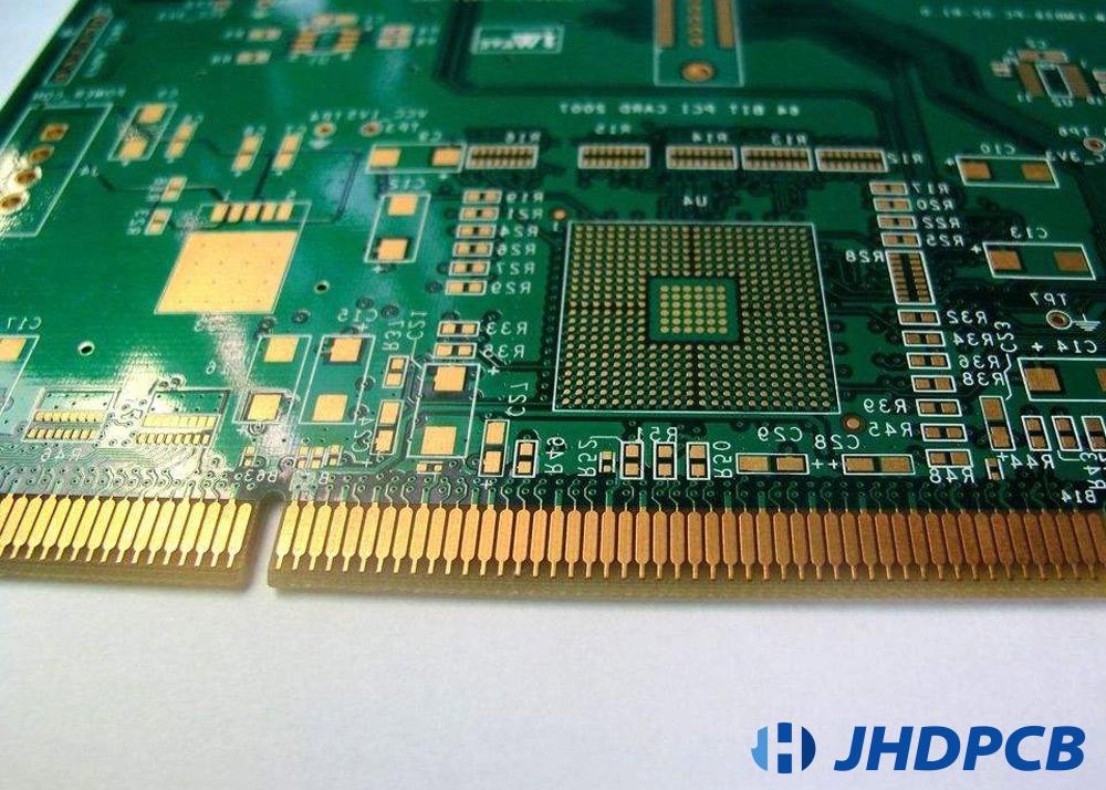
In today’s world of information transmission, signals are sent between numerous devices. The PCB gold finger is responsible for all these connections. Gold fingers have played an important role in interconnecting different devices due to their good electrical conductivity, wear resistance, oxidation resistance and corrosion resistance.
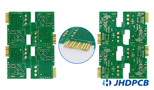
Gold fingers are gold-plated narrow connectors on the edge of the PCB. It is similar to a finger, so we call it a golden finger. Gold fingers are typically between 3 and 50 microns thick. Gold is used for fingers because of its high conductivity and corrosion resistance. The raw material is usually flash gold, sometimes gold is combined with nickel and cobalt to increase wear resistance, as gold fingers need to be inserted and removed frequently. It can effectively protect printed circuit board prototypes from wear and tear.

Processing type of gold finger PCB:
Electroplated Nickel Gold: Due to its superior conductivity, oxidation resistance and wear resistance, it is widely used in gold finger PCBs that require frequent insertion and removal or PCB boards that require frequent mechanical friction. The cost of gold plating is extremely high, and it is only suitable for partial gold plating such as gold fingers. The thickness can reach 3-50u”.
Immersion Gold: Because of its superior conductivity, flatness and solderability, it is widely used in high-precision PCB boards with button positions, BGAs, etc. Gold finger PCBs that do not require high wear resistance can also choose the whole board immersion gold process. The cost of the immersion gold process is much lower than that of the electro-gold process. The conventional thickness is 1u”, up to 3u”.
The electroplating process of the gold finger involves many meticulous steps to ensure that each PCB on the production line is properly configured to transmit the correct signal.
The production process of Goldfinger involves many meticulous steps. The various standards involved in the plating process will help ensure that the gold fingers on each circuit board are perfectly matched to the corresponding sockets on the corresponding motherboard. Every PCB must pass a series of inspections and defect tests. If the gold plating on the board lacks smoothness or does not adhere sufficiently to the surface, it will not be commercially available. JHD’s series of standardized production ensures that every circuit board that rolls off the production line is equipped with the correct equipment to conduct the signal flawlessly.
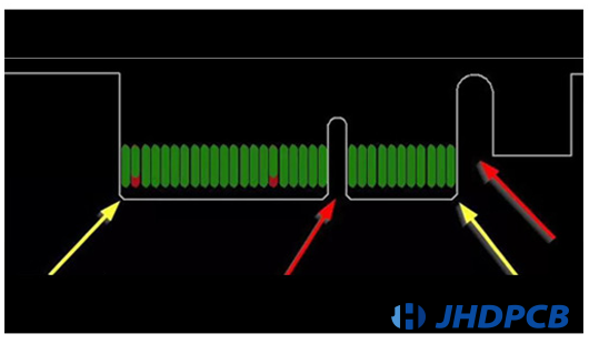
How to Judge Whether There is A Gold Finger On The PCB?
When you see a shape and package similar to the figure below in the PCB design, the first reaction is that the PCB has golden fingers. A simpler method of judging gold fingers: There are PIN devices on both sides of the TOP and BOT of the device, and there will be a U-shaped groove as shown in the figure below.
You are not very familiar with PCB design drawings? It doesn’t matter, JHDPCB has professional engineers for free PCB file inspection. We will professionally inspect your PCB project before putting it into production to avoid unnecessary expenses.
Classification of Goldfinger:
- Conventional gold fingers (flush fingers) are neatly arranged at the edge of the board with rectangular pads of the same length and width. Commonly used in physical objects such as network cards, graphics cards, etc., these golden fingers are more.
- Long and short gold fingers (that is, uneven gold fingers) are located on rectangular pads with different lengths on the edge of the board, which are often used for physical objects such as memory, U disk, and card reader.
- The segmented gold fingers (intermittent gold fingers) are located on rectangular pads with different lengths on the edge of the board, and the front section is disconnected.
Uses of Golden Fingers.
When targeting a fixed computer device, you will see many additional devices connected to the computer itself via PCB gold fingers. Fingers and corresponding slots on the motherboard make connections and upgrades possible. Some of the most widespread uses of golden fingers include:
——External Connection:
Peripherals that have been added to the computer station are connected to the motherboard via PCB gold fingers. Upgrades such as speakers, graphics cards, scanners, printers and monitors all plug into specific slots behind the computer tower. In turn, these sockets connect to a PCB that connects to the motherboard.
——Interconnection Point:
When the secondary PCB is connected to the main motherboard, it is done through one of several female slots, such as a PCI, ISA or AGP slot. Through these slots, the gold fingers conduct signals between peripherals or internal cards and the computer itself.
——Special Adapters:
Goldfinger can add many performance enhancements to a personal computer. With a secondary PCB that plugs vertically into the motherboard, the computer can provide enhanced graphics and high-fidelity sound. Since these cards are rarely attached and reattached individually, gold fingers are usually more durable than the cards themselves.
Some typical applications are:
PCB for memory card reader、Devices that communicate with digital signals (smart watches and smartphones)、Used as a connector to connect external components to the PCB、Used as a connector to connect the daughter board and the computer、Used as a special adapter to increase multiple performances for the computer、Some external devices, such as speakers, scanners and monitors, can be added to the computer with golden fingers、Used as a connection contact in computerized industrial machinery.
Process Rules for PCB Gold Finger.
During the PCB gold finger plating process, the following rules must be followed to make the fingers work properly.
——Design Specifications of Goldfinger:
- Gold fingers should be placed outward from the center of the PCB.
- There shall be no plated through holes (PTH) within 1.0mm of the gold finger.
- The gold finger is at least 1.0mm away from the PCB outline.
- There is no solder mask or screen printing near the gold fingers, the two should be kept at a certain distance.
- The gold fingers must always be facing the opposite direction from the middle of the PCB (if you want the edges to be chamfered).
- Gold fingers need to be chamfered, generally 45°, other angles such as 20°, 30°, etc.
- Immersion tin and immersion silver pads need to be at a minimum distance of 14mil from the top of the finger; it is recommended that the pad should be more than 1mm away from the finger, including via pads.
——Goldfinger Production Specifications:
- Plate thickness of 1.0mm or more.
- Do not spread copper on the surface of the gold finger.
- For PCB boards that need to be plugged and unplugged frequently, in order to increase the wear resistance of the gold fingers, the gold fingers usually need to be plated with hard gold.
- All layers inside the gold finger require copper cutting. Usually, the width of copper cutting is larger than 3mm; it can be used for half-finger cutting and whole-finger cutting. In a PCIE design, all copper that specifies the gold finger should be cut off.
- The gold finger needs to be treated with a whole block of solder mask to open the window, and the PIN does not need to open the steel mesh.
——Production Standard of PCB Gold Finger:
The production standard for PCB gold fingers was formulated by IPC in 2002. In 2015, with the release of IPC A-600 and IPC-6010, the standard was revised again, and the current PCB production IPC standard can be summarized as follows:
Thickness: Gold finger plating thickness should always be in the range of 2 to 50 microinches. Standard thicknesses by size are 0.031″, 0.062″, 0.093″ and 0.125″. Lower thicknesses are typically used for prototypes, while higher thicknesses are used along connecting edges that are regularly inserted, unplugged, and reinserted.
Chemical Composition: For maximum rigidity at the edges of the PCB contacts, the gold plating should contain 5% to 10% cobalt.
Tape Test: To test the adhesion of gold plating to contacts, ICP recommends testing by placing a strip of tape along the edge of the contact. After removing the tape, inspect the tape for traces of plating. If there is significant gold plating on the tape, the plating lacks sufficient adhesion with the contacts.
Visual Test: The visual test that the golden finger should be conducted through a magnifying glass. The edges should have a smooth, clean surface with no unwanted plating or the appearance of nickel.

As technology advances, all standards will be further raised. Therefore, we regularly check with IPC for updates to improve our production standards. JHD will strictly implement standardized, efficient and integrated production for all PCBs and PCBAs to ensure that every order from users to us is fulfilled perfectly. If you want to know more details about gold fingers or other processes in PCB manufacturing, please contact us.


