PCB Layer Direction
What are PCB layer orientations(PCB layer direction)?
Layer orientation is used to help us distinguish between different layers. Many typesetting programs allow mirrored data to be output, which can easily cause manufacturing problems if there are no layer labels or incorrect layer labels. Therefore, identifying each layer with a special label can ensure the correct PCB stack-up and facilitate the correct implementation of the PCB manufacturing process. This rule applies to both prototype PCB assembly and batch PCB production.
Options/controls for layer direction in Altium.
Each signal layer specified in the layer stack is listed in a grid that is displayed in this dialog box. The presentation of each layer is as follows.
- Layer: The name of the signal layer.
- Current Setting: The layer’s currently selected preferred routing direction. This field can be changed. Use the drop-down to select from the following options: Not Used, Horizontal, Vertical, Any, 1 O’Clock, 2 O’Clock, 4 O’Clock, 5 O’Clock, 45 Up, 45 Down, Fan Out and Automatic.
Select the proper layer directions based on how the connecting lines will flow. The Autorouter defines routing paths using topological mapping so that it is not limited to merely routing in the horizontal or vertical direction. It is typically better to have horizontal and vertical outer layers. Set one or more internal layers to have this as the preferred routing direction if, however, the design consists of a multi-layer board with a significant number of connections at a “2 O’Clock” angle. - Actual Direction: The actual wiring direction used by the autowire. This field is read-only. Unless Auto is selected, in which case it will determine the optimal direction to use based on the wiring directions specified for the other layers, it will follow the preferred wiring direction chosen for the layer in the current settings box.
On multi-layered boards, avoid selecting the Any direction option. A layer defined as “any direction” becomes the last resort layer because the Autorouter typically tries to route a connection on the layer whose direction matches it the closest. Only single-sided boards are commonly used with the Any direction option.
Choosing the appropriate direction can have a big impact on routing performance in terms of time and quality because the Layer Patterns pass in a routing strategy uses information about desired routing direction.
It should be noted that angled layers don’t necessarily need to have a partner layer that runs at a 90-degree angle to them because the router will frequently route horizontally or vertically if it wants to avoid an impediment on an angled layer.
Comprehensive understanding of PCB layer direction and precautions.
Orientation of layers information.
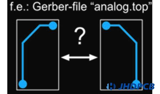
Layer orientation without labels.
Which layer is the TOP layer or the BOT layer, according to you? I’m unsure.
Although the top and bottom layers in your file have been established, as you can see from the diagram, you are still unsure of the layer orientation. This is because almost every CAD program allows mirror output of the data, for both single and multi-layer boards.

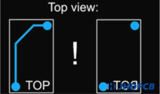
Correct layer orientation labels.
The layer orientation labels should appear in copper, as seen in the diagram, as this is the appropriate layer orientation.
From the top view, the letters “TOP” should be readable and “BOT” is a clear mirror image.

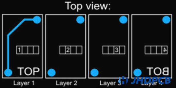
Layer orientation of multilayer boards:
For multilayer PCBs, we should use consecutive labels on each layer so that the orientation of the layers can be easily identified.

Criteria for marking layer orientation:
- It is necessary to produce separate data for the TOP layer and bottom layer.
- Labeling each layer and adding text to the board’s exterior or inside are recommended.
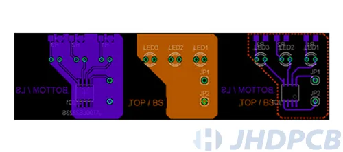
- The letters “BOT” on the bottom layer of the text for the front should be reversed from the top. The PCB will be finished, and “BOT” will be readable.
- Note: The marking text needs to follow the design rules of PCB routing to avoid affecting the wiring.

Notes on stacking under the premise of PCB layer direction.
PCB stackup design is not a simple stacking of layers, where the arrangement of the ground layer is the key, it has a close relationship with the arrangement and direction of the signal. When a multilayer board is compared to a standard PCB, the placement of distinct power and ground layers takes precedence over simply adding the appropriate signal routing layers (copper-laying layers). The benefits of employing power and ground layers instead of the prior power and ground bus are mostly seen in high-speed digital circuit designs.
- Providing a stable reference voltage for the conversion of digital signals.
- Uniformly applying power to each logic device simultaneously.
- Effective crosstalk suppression between signals.
The reason for this is that using a large area of copper as the power and ground layer greatly reduces the resistance of the power and ground. making the voltage on the power layer uniform and smooth, and can ensure that each signal line has a very close ground plane corresponding to it, which also reduces the characteristic impedance of the signal line, can also effectively reduce crosstalk.
If you still have doubts about the direction of the PCB layer, you can contact us at any time. Or send the relevant design documents of the circuit board to our professional engineers for inspection to ensure the smooth progress of subsequent production.
JHDPCB is a leading PCB manufacturer in China, we have more than ten years of PCB manufacturing experience. From simple single-sided PCB to multi-layer PCB or complex HDI PCB. We are committed to delivering high-quality, industry-leading PCBs on time and at a competitive cost.
For more about our advantages, please visit Why choose JHDPCB.


