button plating

Button Plating In Flexible PCB

directory

What is PCB BUTTON PLATING?

PCB button plating, also known as pads-only plating, is a specialized fabrication process used primarily for flexible printed circuit boards (PCBs). This technique involves electroplating copper exclusively onto the vias and small pads that capture the vias, without plating over the entire copper traces on the PCB. The process begins by applying a resist pattern to protect areas around the PCB holes from plating.

After plating the vias and pads, the resist is removed, and the base copper is etched away to create a precise pattern featuring raised button-like areas. This method is essential for maintaining the flexibility of the PCB while ensuring robust electrical connectivity and durability at the contact points. The resulting board has a distinctive flat surface with elevated areas resembling buttons, hence the name “button plating.” By using a button plate in this process, manufacturers can achieve the desired pattern and functionality required for advanced electronic applications.

What exactly is a Flex PCB?

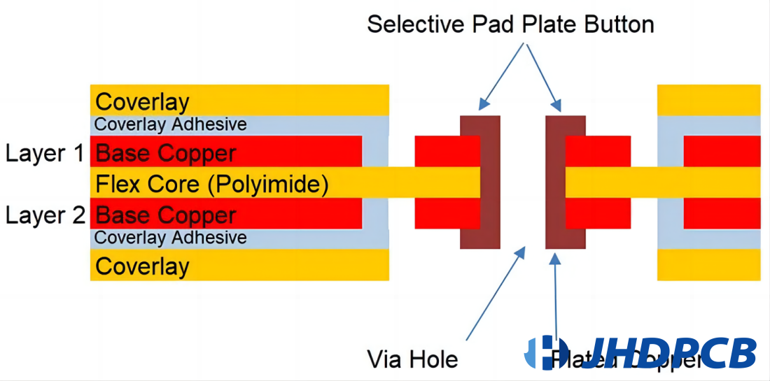
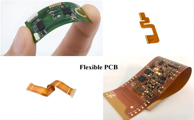
A flexible printed circuit board (flex PCB) is a specialized type of printed circuit board designed to be both flexible and bendable. Unlike traditional rigid PCBs, which use a hard, inflexible substrate, flex PCBs are constructed from thin, pliable materials such as polyimide or polyester. This flexibility allows the PCB to bend, fold, and conform to various shapes and contours, making it ideal for use in compact and dynamic electronic devices. Flex button plating techniques, which involve selectively applying conductive coatings onto specific areas of the flex PCB, further enhance its functionality by ensuring reliable electrical connections even in areas subject to bending and movement. This combination of flexibility and precise button plating is crucial for maintaining durability and performance in modern electronic applications.

flexible PCB plating

The manufacturing process for flex PCBs shares similarities with that of rigid PCBs but involves key differences. Instead of using a rigid substrate, a flexible material is used. The circuitry on a flex PCB is typically printed using specialized inks or conductive pastes, which are applied to the flexible substrate through a precise printing process. To enhance the performance and durability of these circuits, flexible PCB plating is employed. This plating process ensures that the conductive layers on the pliable surface are robust and reliable, enabling the creation of intricate and durable circuits that can withstand dynamic flexing and bending.

In applications involving PCB button plating, flex PCBs play a crucial role. Button plating refers to the process of applying a conductive coating—usually gold or nickel—onto specific areas of the PCB, such as where push-buttons or connectors are located. This plating enhances the electrical conductivity and reliability of the button interfaces, ensuring consistent performance even under bending or stress. By integrating button plating into flex PCBs, designers can achieve both flexibility and high performance, creating robust electronic devices that maintain functionality in varying physical conditions. The use of gold plated buttons in these designs further enhances the durability and conductivity of the button interfaces, providing a reliable solution for demanding electronic applications.

When and where are PCB button plating needed?

Application Area Need for Button Plating Benefits
Consumer Electronics Remote controls, game controllers, keyboards Enhances durability and conductivity of contacts; withstands frequent use; resists corrosion and wear
Industrial Sector Machinery and equipment operating in harsh conditions Provides stable electrical connections; withstands high vibration and extreme temperatures
Automotive Sector Automotive controls and interfaces Ensures reliable connections in high-vibration environments; durable performance
Medical Devices Devices requiring precise and reliable performance Consistent electrical conductivity; supports device functionality while ensuring safety
Aerospace & Defense Aerospace and defense equipment Reliable and rugged connections; critical performance under extreme conditions
Specialized Technologies Applications requiring specific deposit configurations (e.g., plated through holes) Targeted plating; avoids unnecessary weight or complexity

PCB button plating serves a crucial role in various electronic applications where reliable and durable electrical connections are essential. One of the primary uses of button plating is in devices requiring user interfaces, such as remote controls, game controllers, and keyboards. These applications rely on button plating to enhance the durability and conductivity of the contacts that users interact with daily. By using a plate button approach in these interfaces, manufacturers can ensure that the electrical connections remain robust and efficient even with frequent use.

In environments where frequent use can lead to wear and tear, like remote controls, button plating ensures that the contacts inside buttons remain robust and efficient over time. By applying a thin layer of metal through this process, the contacts become more resistant to corrosion and wear, thereby extending the lifespan and reliability of the electronic device.

Beyond consumer electronics, button plating finds critical applications in industrial and automotive sectors. These industries demand stable electrical connections capable of withstanding harsh conditions such as high vibration and extreme temperatures. Button plating provides a solution by creating strong, long-lasting connections that are less prone to failure compared to traditional contact methods.

Medical devices also benefit from button plating, where precise and reliable performance is crucial. The process ensures consistent electrical conductivity, supporting the device’s functionality without compromising on safety or usability. Similarly, in aerospace and defense applications, where reliability and ruggedness are paramount, button plating offers a dependable solution for creating durable electrical contacts.

Moreover, the versatility of button plating extends to specialized technologies requiring specific deposit configurations. For instance, in applications where only the plated through holes (PTHs) and supporting pads require heavy deposition, button plating allows for targeted plating without adding unnecessary weight or complexity to the PCB design.

In summary, PCB button plating is indispensable in scenarios demanding enhanced electrical conductivity, durability, and reliability. Its application spans across a wide spectrum of industries, from consumer electronics to medical devices and industrial machinery, where consistent performance under challenging conditions is non-negotiable. By leveraging button plating, manufacturers ensure that their products meet stringent performance requirements while maintaining cost-effectiveness and operational efficiency.

What Are the Applications of Button Plating?

Applications of Button Plating

Button plating is a specialized technique utilized in two critical applications within the electronics industry:

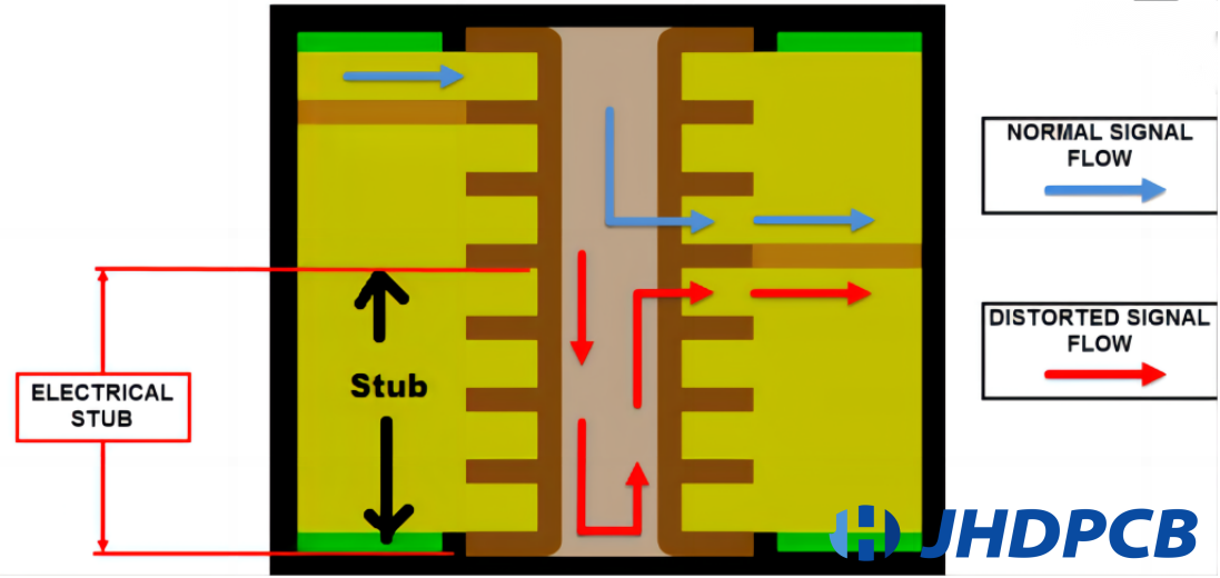
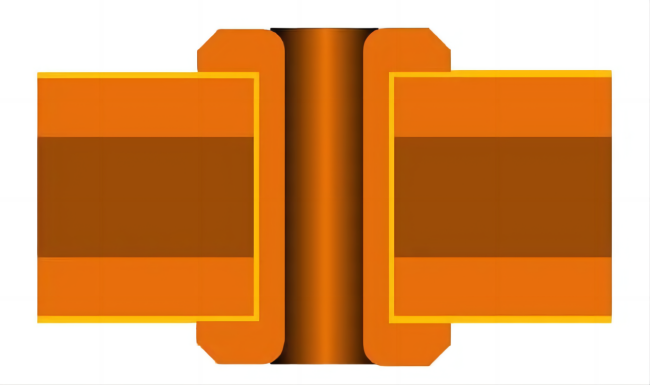
In scenarios where flexible circuits are subjected to frequent bending or flexing, such as in portable devices (e.g., laptops) or mechanical assemblies (e.g., disk drives), button plating plays a crucial role. Unlike conventional electroplating, which deposits copper uniformly across the entire surface of the circuit, button plating selectively deposits copper only on designated areas, typically the contact pads or terminals. This selective plating approach avoids adding additional copper to the circuit traces themselves.

The rationale behind this lies in the differences between electroplated copper and rolled annealed copper. Electroplated copper tends to have a grain structure that is less flexible compared to the rolled annealed copper used in the base material of flexible circuits. This difference can result in increased susceptibility to cracking or fracturing when the circuit undergoes repeated bending. By minimizing electroplated copper through button plating, manufacturers can significantly enhance the durability and longevity of flexible circuits, ensuring they can withstand the expected number of flex cycles over the product’s lifetime.

Furthermore, optimal design practices complement button plating to further improve flex life. These practices include using rolled annealed copper with grain direction parallel to the roll length, positioning the circuit layout to orient the grain direction perpendicular to the flex plane, and ensuring a balanced material thickness to avoid compression or tension on the copper during bending. Thinner copper layers are also preferred for improved flexibility.

In high-speed electronic applications where signal integrity is paramount, maintaining consistent impedance throughout the circuit is crucial. Button plating addresses the challenge of variability in copper thickness that can occur during conventional electroplating processes. Electroplated copper thickness can vary due to factors like current density fluctuations, resulting in impedance variations that can affect signal transmission quality.

Impedance Control Application

By selectively plating only the necessary areas (such as pads or critical signal paths) with button plating, manufacturers can mitigate these variations. This approach helps achieve more uniform impedance characteristics within individual circuits and across multiple production batches. Consistency in impedance is further supported by using homogeneous dielectric materials, ensuring equivalent spacing between ground planes, and maintaining uniform copper thickness and spacing.

Additionally, the choice of materials and construction techniques, such as adhesiveless laminates for dielectric layers, helps minimize impedance variations caused by differing dielectric constants of adhesives.

In essence, button plating is a key technique that improves both the mechanical durability and electrical performance of flexible circuits and high-speed electronic designs. Flexible button plating addresses specific challenges related to mechanical durability in dynamic flex applications and impedance control in signal integrity-sensitive environments. This technique contributes to overall product reliability and longevity by ensuring robust electrical connections and maintaining performance in flexible, high-demand conditions.

What is the Benefit of PCB Button Plating?

PCB button plating offers significant advantages that address specific challenges in electronic design and manufacturing, making it a preferred choice in various applications.

One of the primary benefits of PCB button plating is its ability to maintain the flexibility of flexible PCBs (Flex PCBs). Unlike traditional methods that involve plating over the entire copper surface, button plating selectively deposits metal only on the vias and pads. This targeted approach preserves the PCB’s flexibility, crucial for applications requiring frequent bending or movement, such as wearable devices and flexible displays.

For high-speed electronic devices, maintaining precise impedance control is critical to ensure signal integrity and performance. Button plating supports homogeneous base copper, allowing for more accurate impedance matching across the PCB. This capability is essential in applications like telecommunications, where signal quality and reliability are paramount.

In the quest for smaller and more compact electronic devices, PCB button plating plays a vital role. By reducing the width and spacing between traces, button plating enables the creation of PCBs with tighter geometries. This advancement is particularly beneficial in industries such as mobile devices and IoT sensors, where space constraints drive the need for miniaturization without compromising functionality.

Button plating offers a cost-effective solution compared to alternative methods, especially in flexible PCB manufacturing. By avoiding unnecessary plating on copper traces, companies can optimize material usage and reduce production costs. This efficiency is crucial for achieving competitive pricing in consumer electronics and industrial applications.

The versatility of PCB button plating extends to various applications beyond consumer electronics. It is widely used in automotive, medical, and aerospace industries where reliability, durability, and performance are paramount. Whether it’s enhancing the robustness of controls in automotive systems or ensuring precise signal transmission in medical devices, button plating provides a tailored solution to meet specific industry requirements.

The protective layer provided by button plating improves the environmental resilience of PCBs, shielding them from corrosion and mechanical wear. This durability enhances the lifespan of electronic devices, reducing maintenance needs and enhancing overall reliability.

In conclusion, PCB button plating offers a blend of technological advancements and practical benefits that cater to modern electronic design challenges. From enhancing flexibility and impedance control to supporting miniaturization and reducing costs, button plating remains an indispensable process in the evolution of electronic devices across diverse industries. Its ability to optimize performance while meeting stringent design specifications makes it a preferred choice for engineers and manufacturers striving to innovate in today’s competitive market landscape.

The Difference Between Panel Plating and Button Plating in PCB Manufacturing

The Difference Between Panel Plating and Button Plating in PCB Manufacturing

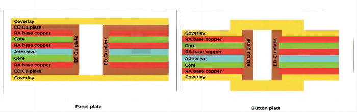
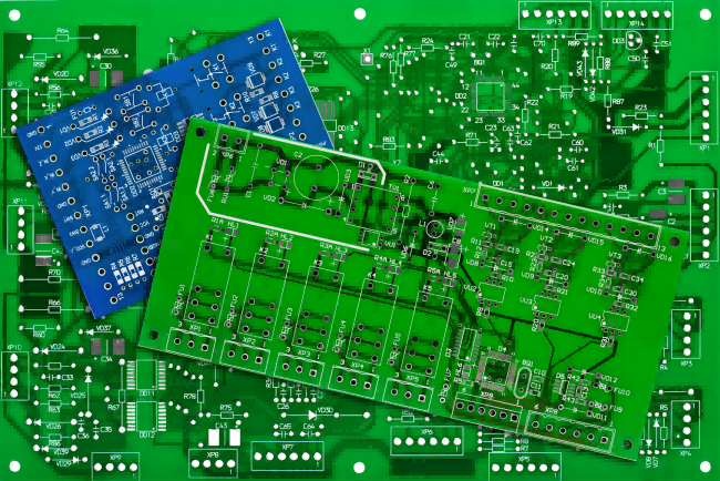
In PCB (Printed Circuit Board) manufacturing, selecting between button plating vs. panel plating significantly impacts the board’s performance and characteristics. Each method has distinct applications and benefits tailored to specific design needs.

Panel Plating

Panel Plating involves uniformly depositing copper across the entire surface of the PCB panel, including all vias and through-holes. This method builds up a consistent layer of metal on both sides of the substrate, typically before any imaging or etching steps. The advantages of panel plating include:

  • Uniform Copper Thickness:
    The even copper deposition minimizes variation in current density across the board, ensuring consistent conductivity.
  • Robust Conductivity:
    The thick copper layer enhances the board’s ability to carry current, making it suitable for high-power applications.

However, panel plating also presents some drawbacks:

  • Material Waste:
    A significant amount of copper is deposited only to be etched away during the imaging process, leading to increased material usage and cost.
  • Reduced Flexibility:
    The added copper can make the PCB less flexible, potentially causing issues in designs requiring frequent bending or dynamic flexing.
  • Impedance Variability:
    The additional copper can affect controlled impedance applications, where precise impedance control is crucial.

Panel plating is often favored for its simplicity and effectiveness in applications where a uniform copper thickness and structural integrity are essential, but it may not be ideal for flexible or high-precision designs.

Button Plating

Button Plating, or “pads only plating,” is a more targeted approach. In this method, a plating resist is applied to cover the entire panel except for specific areas, such as vias and small pads where copper is needed. The key features of button plating include:

  • Selective Plating:
    Copper is only deposited on the vias and pads, reducing overall copper thickness and preserving flexibility in the PCB. This is particularly important in processes involving button plating via.
  • Enhanced Flexibility:
    By avoiding the uniform deposition of copper across the entire board, button plating maintains better flexibility, making it suitable for applications involving dynamic flexing or tight bend radii.
  • Controlled Impedance:
    With minimal additional copper on traces, impedance control is more manageable, making this method advantageous for high-speed or high-frequency applications.

Button plating involves a more complex process with additional imaging and resist steps, which can increase production costs. However, the benefits in terms of flexibility and impedance control often outweigh these costs for designs with specific requirements.

Choosing Between Panel and Button Plating

The choice between button plating vs. panel plating depends on the specific demands of the PCB application. Each technique offers unique advantages that cater to different design requirements and performance criteria.

  • Panel Plating:
    Best for standard PCBs where uniform copper thickness and structural strength are critical. It is a cost-effective choice for applications where flexibility and precise impedance control are not primary concerns.
  • Button Plating:
    Preferred for flexible PCBs or HDI (High-Density Interconnect) designs that require reduced thickness and enhanced flexibility. It is ideal for high-speed electronic applications or those with dynamic flexing needs. 

Considerations for Designers

Designers should weigh the implications of each plating method on the final PCB’s performance:

  • Panel Plating: Offers robust conductivity and structural integrity but may limit flexibility and add material costs.
  • Button Plating: Enhances flexibility and maintains impedance control but involves higher production complexity and cost.

FAQ of Button Plating

Copper trace plating is crucial in flex circuits for PCB button plating because it enhances the durability and conductivity of the electrical paths. The plating process ensures that the copper traces are protected against oxidation and wear, which is essential for maintaining reliable connections in dynamic flex applications where the circuit is regularly bent and flexed.

The bend radius significantly impacts the performance of flex circuits in PCB button plating applications. A smaller bend radius can increase the stress on the copper traces and the plated surfaces, potentially leading to cracks or breaks. Ensuring an appropriate bend radius helps maintain the integrity and functionality of the plated copper and the overall flex circuit.

The grained structure of copper affects the mechanical properties and reliability of PCB button plating. A fine and uniform grain structure can enhance the durability and flexibility of the copper, reducing the likelihood of cracks or failures under stress. This is especially important in dynamic flex applications where the material is subject to repeated bending and flexing.

Surface finishes in PCB button plating offer several advantages, including improved solderability, enhanced corrosion resistance, and better electrical conductivity. Surface finishes like ENIG (Electroless Nickel Immersion Gold) or OSP (Organic Solderability Preservatives) help protect the base copper and ensure reliable performance of the button contacts.

Base copper thickness plays a critical role in the PCB button plating process. Thicker base copper can provide better current carrying capacity and improved thermal management. However, it also requires careful control during the plating process to ensure even deposition and avoid issues like excessive plating buildup or uneven surfaces.

Impedance control is crucial in PCB button plating for high-frequency applications to ensure signal integrity and minimize signal loss. Proper impedance matching can prevent reflections and distortions in the signal, which is vital for maintaining the performance of high-speed digital circuits and ensuring reliable communication.

Pads-only plating refers to a selective plating process where only the contact pads are plated, leaving the rest of the board surface unplated. This approach is used when specific areas, such as button contacts, require enhanced durability and conductivity without adding unnecessary weight or complexity to the entire board.

The thickness of plated copper directly impacts the performance and durability of PCB button plating. Thicker copper plating can provide better wear resistance and improved electrical conductivity, which is essential for reliable button contacts. However, it also requires precise control to avoid issues like excessive buildup that can affect the fit and function of the components.

In conclusion, effective PCB button plating is essential for ensuring the longevity and reliability of electronic devices. As technology advances, the need for precise and high-quality plating processes becomes even more critical. At JHDPCB, we understand the complexities involved and are well-equipped to meet these demands. Our expertise in PCB manufacturing, combined with advanced plating technologies and a commitment to quality, positions us as a leader in the industry. Whether you need innovative solutions or reliable production, JHDPCB is your trusted partner for all your PCB button plating needs.

Get a PCB Quote Now

Open high-quality PCB manufacturing services in JHDPCB

Leave a Comment