copper balancing

Copper Balancing In PCB Manufacturing

directory

What is copper balancing in PCB?

Copper balance in PCB (Printed Circuit Board) fabrication refers to the symmetrical distribution of copper traces across each layer of the board’s stack-up. This method is crucial for maintaining the electrical and mechanical stability of the PCB, as it helps prevent issues such as board warping, twisting, or bowing.

In a well-designed PCB, the top half layers are mirrored with the bottom half layers, ensuring an equal distribution of copper on both sides. This balance is essential because copper plays a vital role in signal transmission and heat dissipation due to its excellent electrical and thermal properties. When used as traces, copper transfers heat along with the signal across the board, reducing damage caused by irregular heating that could lead to internal track breakage.

Additionally, copper can be utilized as a heat sink layer for power-generating circuits, eliminating the need for extra heat sink components and significantly reducing manufacturing costs. Furthermore, when copper is plated on the PCB, it increases the thickness of conductors and surface pads, while also providing a strong inter-layer connection through plated through holes.

Overall, achieving copper balance in PCB fabrication is critical for enhancing the manufacturability, performance, and production yield rate of the board. Copper balancing pcb ensures consistent copper coverage in every layer, preventing potential electrical and mechanical problems that could impede circuit performance.

What's the role of copper balancing?

Copper balancing is an often overlooked but crucial step in printed circuit board (PCB) fabrication. At its core, copper balancing involves the even distribution of copper layers throughout the PCB’s stack-up to ensure that the board does not experience any deformations such as bowing, twisting, or warping. This meticulous process influences several key aspects of PCB manufacture and performance:

  • Preventing Board Deformation
    When copper is unevenly distributed, it can lead to stress points within the PCB structure. These stresses can manifest as bow, twist, or warp, especially during thermal cycles experienced in soldering or reflow processes. A well-balanced copper layout ensures that stresses are minimized, keeping the board flat and enhancing the accuracy of automated assembly processes.
  • Maintaining Integrated Thickness
    The thickness of the PCB after lamination depends greatly on the distribution of copper in each layer. Uneven copper can result in variations in the final board thickness, affecting both the look and the fit of the PCB in its intended enclosure or application. Copper balancing helps to maintain consistent thickness across the entire board.
  • Ensuring Optimal Electrical Performance
    Electrical properties, like impedance and conductivity, rely on the consistent behavior of the PCB materials. Copper balancing helps standardize these properties because it ensures a predictable copper distribution. This consistency is vital for applications where precise control over electrical characteristics is required.
  • Promoting Heat Dissipation
    Copper is an excellent conductor of heat, so balanced distribution aids in the dissipation of heat generated by components and current flow. This can prevent hotspots that could otherwise degrade the PCB or reduce the lifespan of components. In high power applications, using copper to distribute heat more effectively can negate the need for additional heat management strategies.

In summary, the role of copper balancing is to provide a robust foundation for PCB reliability and functionality. It ensures that the mechanical and electrical properties of the board remain uniform and predictable, safeguarding against issues that may arise from irregular copper distribution. By prioritizing copper balance during the design phase, manufacturers can avoid costly reworks and produce PCBs with superior performance and longevity.

Optimizing Copper Balance in PCB Fabrication: Factors and Impacts

The integrity and performance of Printed Circuit Boards (PCBs) rely heavily on the precise control of copper balance during the fabrication process. Copper serves as the primary conductor of electricity within PCBs, making its consistent distribution and thickness across the board vital for ensuring efficient signal transmission, effective thermal management, and long-term reliability. However, achieving an optimal copper balance is a complex task that involves managing several critical factors.

Panel Region Copper Thickness (μm)
Center 35.2
Top-Left 33.8
Top-Right 34.5
Bottom-Left 36.1
Bottom-Right 35.7

The table above highlights the challenge of maintaining uniform copper thickness across different regions of a PCB panel. The copper thickness variation—ranging from 33.8 μm to 36.1 μm across the edges and corners compared to the desired 35.2 μm at the center—can lead to differences in electrical resistance and impedance. These variations can cause signals to degrade over certain paths, leading to potential data losses or inaccuracies in high-speed electronics. Moreover, non-uniform copper distribution can result in uneven heating, which may shorten the PCB’s lifespan due to thermal stress.

Plating Time (minutes) Copper Thickness (μm)
60 32.5
65 34.8
70 37.2
75 39.6

The direct relationship between plating time and copper thickness, as shown in above Table, underscores the importance of controlling the plating process. Inadequate plating time leads to under-plated areas, which have reduced conductivity and increased resistance, while over-plating can result in wasted material and potential short circuits if the copper thickness exceeds specified tolerances. Precise timing and process controls are necessary to achieve the desired copper thickness, avoiding these pitfalls.

Current Density (A/dm²) Plating Rate (μm/min)
2.0 0.42
2.5 0.55
3.0 0.68
3.5 0.79

The third table emphasizes the influence of current density on the copper plating rate. Variations in current density during plating can result in uneven copper deposition, further contributing to thickness non-uniformity. Maintaining a consistent current density throughout the plating step is crucial to ensure an even plating rate. Control parameters such as bath composition, agitation, and temperature must be closely monitored to maintain optimal plating conditions.

Furthermore, other factors such as the type of plating solution, anode quality, and plating chemistry also play significant roles in achieving the desired copper balance. Minor changes in the plating bath chemistry, including pH levels and additive concentrations, can significantly affect the copper’s physical properties and plated thickness. Proper maintenance and frequent analysis of the plating solution are essential to prevent chemical imbalances that could lead to substandard plating results.

In conclusion, optimizing copper balance in PCB fabrication requires meticulous attention to detail and precision in process control. Manufacturers must adopt rigorous quality control measures, utilize advanced plating technologies, and implement regular monitoring to ensure consistent copper distribution. By understanding and mitigating the impact of factors such as panel region variability, plating time, and current density, manufacturers can produce high-reliability PCBs that meet stringent performance standards for today’s demanding electronic applications.

What will happen without PCB Copper Balance?

Without proper PCB copper balance, a series of mechanical and electrical issues can arise during both the fabrication process and subsequent assembly of the printed circuit board (PCB). Here’s a detailed explanation of the potential problems:

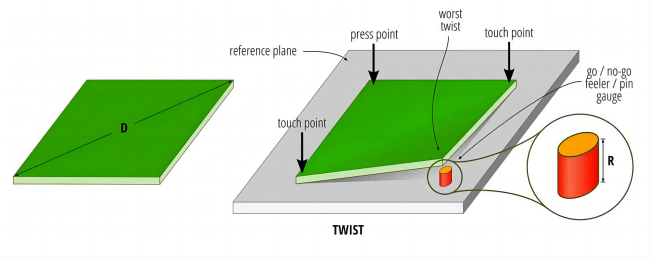
  • Twists: An uneven distribution of copper can cause one corner of the PCB to be displaced vertically, not lying in the same plane as the other three corners. This is known as a twist and can lead to misalignment during component placement or soldering.

    Mechanical Alignment Issues twists

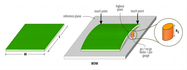
  • Bow: Unbalanced copper can result in a spherical or cylindrical curvature where the four corners of the board remain in the same plane but the center is curved. This bowing can also cause alignment issues during manufacturing.

Mechanical Alignment Issues bows

  • Warp: Irregular copper distribution, coupled with the high temperatures and pressures of the fabrication process, can cause the PCB to warp, leading to what is often referred to as the “potato chip” effect. Warpage can stress traces and solder joints, potentially damaging circuits.

If the stack-up is not balanced, there can be a mismatch in thickness on different sides of the board after lamination. This can affect the fit of the PCB into its intended enclosure or application, as well as the reliability of connections to components. 

Inconsistencies in copper coverage between layers can lead to variability in electrical properties such as impedance and conductivity. This can compromise signal integrity and overall circuit performance, especially in high-frequency applications where precise control over these parameters is critical.

Copper’s ability to distribute heat is hindered when it is not evenly distributed. This can lead to hotspots that may degrade the PCB or reduce the lifespan of components, particularly in high-power applications.

Boards that warp or twist can stress the metal traces, leading to breaks that are difficult to detect and diagnose. Solder joints under stress due to warpage can result in intermittent problems or open circuits, increasing the likelihood of manufacturing defects and associated costs.

Without proper copper balance, the larger the board and the more layers it contains, the more likely it is to warp. This can limit the size and complexity of PCBs that can be reliably manufactured.

Mechanical alignment issues can cause stoppages on automated assembly lines, where precise component placement is required. This downtime can be costly and impact production efficiency.

In summary, without proper PCB copper balance, manufacturers risk mechanical deformations, variations in thickness, electrical performance issues, heat dissipation problems, increased manufacturing defects and costs, limitations on board size and complexity, and potential assembly line stoppages. These issues underscore the importance of maintaining copper balance pcb a balanced copper distribution throughout the PCB layer stack-up to ensure reliable and efficient manufacturing and performance of PCBs.

How to Achieve PCB copper balancing?

Printed Circuit Boards (PCBs) are intricate assemblies of insulating substrates adorned with copper tracks and electrical components. Ensuring copper balance within a PCB is crucial for optimal performance and manufacturability. Here’s a detailed exploration of how to balance copper and strategies to achieve PCB copper balancing:

    • Layer Configuration:
      To begin with, create a new CAD project with three layers designated for specific components of the PCB. Layer 0 is allocated for the board outline, which serves as a reference for the overall dimensions and layout of the PCB. This layer helps designers visualize the physical boundaries within which they need to place electronic components and interconnecting copper tracks.
    • Front Side Copper Tracks:On layer 1, designers draw the copper tracks that will be located on the front side of the PCB. These tracks serve as pathways for electrical signals and connectivity between various electronic components mounted on the board. To calculate the area occupied by these tracks, designers multiply the track width by its length. For instance, if a track has a width of 0.02 inches and a length of 1.5 inches, the total area covered by that track would be 0.03 square inches. Accurately calculating the area helps in determining the amount of copper needed and contributes to maintaining balance during the design process.
    • Back Side Copper Tracks:

      Layer 2 is dedicated to the copper tracks on the back side of the PCB. Designers should aim to balance the copper area on this layer with that of the front side (layer 1). This means that the cumulative area of all tracks on both layers should be approximately equal. Balancing the copper area ensures that the PCB has uniform thermal and electrical properties across both sides, reducing the risk of warping or other structural issues that can arise from uneven copper distribution. When sending the finalized CAD design to the manufacturer, it is essential to specify equal copper weight for both sides of the board. This instruction guarantees that the manufacturer will produce a PCB with balanced copper distribution, enhancing its overall performance and reliability.

Layer Stackup of copper balancing

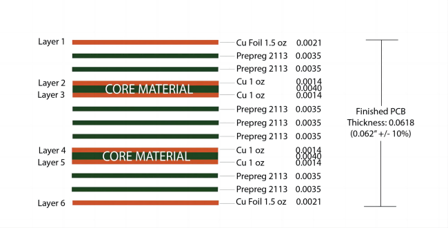
  • Symmetrical Configuration:
    When designing the layer stackup, it is important to aim for symmetry by placing dense copper layers at the center of the board and working outward in a symmetrical manner. This means that if a particular layer has a certain amount or distribution of copper, its counterpart on the opposite side of the board should mirror that as closely as possible. Symmetry in layer configuration helps to balance the thermal expansion and contraction properties of the board, which can reduce warping and improve overall signal integrity. It also makes the manufacturing process more straightforward, as asymmetrical designs can lead to handling issues during production.
  • Power Planes:Maintaining symmetrical power planes throughout the stackup is another key aspect of layer stackup. Power planes are large areas of copper used to distribute power evenly across the PCB. These planes should be symmetrically arranged and have equal copper weights to preserve signal integrity and control impedance. Impedance control is particularly crucial for high-speed and high-frequency applications where signals are more sensitive to variations in the PCB’s physical characteristics. By keeping power planes symmetrical, designers can ensure that the board’s electrical performance remains consistent and predictable.
  • Copper Pour:On signal layers where there is not enough metal to achieve the desired copper density, designers can add copper pours to increase the density. Copper pours refer to areas of copper that are added to fill in spaces between traces and other components, typically on layers without a continuous ground or power plane. Cross-hatched metal fill areas are an effective way to balance copper distribution, as they help to minimize variations in impedance caused by uneven copper coverage. This technique ensures uniform electrical performance across the board while also providing additional mechanical stability.
  • Central Layer Design:
    The central layer of the PCB should be designed with maximum copper thickness, and the remaining layers should be balanced accordingly. This approach helps to prevent the “potato chip effect,” which is a phenomenon where an uneven distribution of copper on different layers causes the board to bend or warp. By concentrating more copper in the center and balancing the surrounding layers, the overall structural integrity of the PCB is maintained, reducing the risk of manufacturing defects and performance issues.
  • Grid Design:
    For wide copper areas, implementing grids instead of solid planes can prevent copper density mismatches and minimize bow and twist issues. Grid designs involve creating patterns of small, interconnected copper squares or lines that distribute copper evenly across the PCB. This approach enhances the board’s structural integrity and manufacturability by ensuring that there are no large, solid areas of copper that could cause imbalances during production or use.

Circuit Grid Design

  • Symmetrical Power Planes:
    Power planes should be placed symmetrically within the layer stackup and maintain uniform copper weight to ensure balanced power distribution. This practice reduces electromagnetic interference (EMI) and improves the reliability of power delivery across the PCB. By keeping power planes symmetrical and maintaining consistent copper weights, designers can ensure that the board’s electrical performance remains stable and predictable.
  • Core and Prepreg Layers:
    Maintaining uniform copper proportion in core and prepreg layers is essential for upholding overall PCB copper balance. These layers, which form the foundation of the PCB, must have consistent copper distribution to minimize material stress and enhance thermal conductivity. Proper copper balance in these layers contributes to the longevity of the PCB by ensuring that heat is dissipated effectively and that the board remains stable under various operating conditions.

Achieving PCB copper balancing involves meticulous planning and execution throughout the design and manufacturing stages. By adhering to symmetrical layer stackups, strategic copper distribution, and careful consideration of copper weight and thickness, designers can produce PCBs with optimal performance, reliability, and manufacturability.
Implementing these practices not only enhances PCB functionality but also minimizes manufacturing challenges, ensuring the highest yield and quality in PCB production. By prioritizing copper balancing, designers can deliver robust and efficient PCBs that meet the demands of modern electronic applications.

Q&A of Copper Balancing

An imbalance in copper distribution can lead to uneven heating during reflow soldering, potentially causing solder joint defects or failures. Balancing the copper helps maintain consistent heat distribution, ensuring reliable solder joints.

The potato chip effect refers to warpage in PCBs caused by uneven internal stresses, resembling the curvature of a potato chip. Copper balancing helps to reduce internal stresses by distributing copper evenly, minimizing this type of warpage.

Excess copper can lead to an imbalance in the copper distribution, causing issues with thermal management, signal integrity, and mechanical stability. Copper balancing involves managing this excess copper to maintain optimal performance.

Techniques such as using circles, squares, or solid shapes for copper filling help to balance the copper load. These shapes can be strategically placed to manage thermal dissipation and electrical performance, enhancing overall PCB design effectiveness.

Copper balancing in PCB design and fabrication offers several advantages, including improved signal integrity by reducing crosstalk and reflections, enhanced thermal management to prevent hotspots and extend component life, increased mechanical stability to minimize warpage and delamination, better electrical performance through consistent impedance and reduced EMI, and overall improved reliability and performance of the board. Proper copper balancing also facilitates more efficient manufacturing processes and can lead to cost savings by reducing the number of iterations needed to achieve a stable and reliable design.

In conclusion, copper balancing in PCB design is a crucial aspect that cannot be overlooked. It ensures proper electrical functionality and prevents issues such as signal interference and power supply noise. By achieving a balanced copper distribution, designers can enhance the overall performance and reliability of their circuit boards.

At JHDPCB, we understand the importance of copper balancing and have extensive experience in delivering high-quality PCB designs with optimal copper distribution. Our team of experts utilizes advanced software tools and techniques to ensure precise copper balancing for all our clients’ projects. If you have any questions or require assistance with your PCB design needs, feel free to consult us. We are always here to help bring your electronic ideas to life!

Get a PCB Quote Now

Open high-quality PCB manufacturing services in JHDPCB

Leave a Comment