Comprehensive understanding of PCB power design

sales@jhdpcb.com
directory
Get to know PCB power supplies. and its importance.
In PCB Power applications, no matter what power supply method the device uses, a circuit needs to be designed to regulate the power supply to the device. Large amounts of current must be conducted for equipment to function properly without affecting efficiency and losing power.
At the same time, with the increase of circuit design density and complexity, the complexity of power supply design also increases. Designing a power supply that can provide the required power to each PCB component (transmitter, IC, capacitor, etc.) is a challenging task for the PCB designer, as each component has different power requirements. Only a perfect power supply design can meet the normal operation of subsequent PCB schematics, design layout and manufacturing to use.
Power PCB design begins by calculating the trace width and maximum current threshold that the power PCB should handle. Second, the power PCB design should also include proper material selection that can control the heavier components.
Not only should the board hold the weight, it should also be held in place with maximum grip so that in the case of control knobs, high-power relays, and heavy-duty cable connectors, blunt physical forces won’t damage the PCB.
Typically, power electronic circuits require low resistance paths and high current carrying capabilities. As a result, some power converters have to deal with disturbances and noise due to high-traffic, high-speed switching that affects the rest of the analog and digital circuits.
At the highest voltages, particular attention is paid to thermal management issues arising from high-power electronics and necessary safety features. Such as grounding, power isolation, heat dissipation and electrostatic discharge. Power supply PCBs should consider power and signal integrity issues, because of the way ICs operate, signal and power integrity are closely related, and some power supplies can generate significant radiated EMI that affects other parts of the board. Systems without or connected to power are immune to signal integrity or power integrity issues, But implementing some necessary impedance design procedures can help prevent redesign. IPC® regulates the safety features of the power supply PCB. Consumer electronics products should include top-level security features to keep users safe.
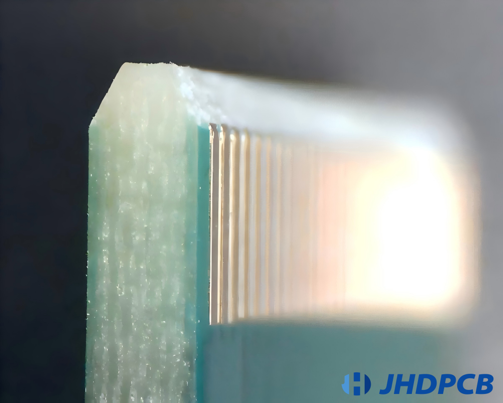
Power PCB designs typically use a high thickness copper grater or equal to 2oz. However, solder bridges are required in many cases to provide adequate current-carrying capacity. Spark gaps are often included to prevent circuit damage from the ark.
PCB Power Design Power Type.
The first step in building a PCB power supply is to choose the type of power supply that is suitable for use in your device or project. Unregulated power supplies are the first choice for converting AC power from a wall outlet to DC voltage. The output of this power supply will contain a ripple waveform because the output is not smoothed with a voltage regulator. Modern applications often use regulated power supplies to minimize ripple.
There are two main options for regulating the DC output of a power supply: linear regulators and switch-mode power supplies.
Linear regulators— Are very low noise, but they tend to be bulky due to the use of heat sinks or other active cooling measures required for thermal management. The remarkable heat dissipation of these power supplies is excellent.
Switch-mode power supplies— offer higher efficiency over a wider current range, allowing these power supplies to be used in smaller form factors. However, these power supplies use a PWM circuit to smooth and regulate the output voltage, which requires the use of active switching elements (usually MOSFETs). This means that the system radiates strong EMI. This switching noise will appear as a ringing signal (i.e. conducted EMI) at the output and needs to be filtered from the output.
Considerations for PCB power supply design:
Due to the increased density and complexity of PCB power supply design. PCB power supply is not limited to power conversion, and ensuring power integrity and heat dissipation performance in power output is also a consideration in PCB power supply design. PCB designers have more customization options for PCB power design and layout. Designers must follow certain rules to help deal with common problems associated with them, such as: including EMI, designing traces to handle high currents, reducing current loops, component selection, and following datasheet layouts.
Some important things are listed below:
Selecting Voltage Regulators for PCB Power Design:
There are two options when choosing a power regulator, linear regulators and switch mode regulators. Linear regulators provide low noise output but dissipate more heat and require a cooling system. Switch-mode regulators are very efficient over a wide current range, and it is easy to control the output voltage of the switching regulator by adjusting the duty cycle of the PWM signal that controls the switching action.
Linear mode requires— the input voltage to be higher than the desired output voltage, which makes the linear regulator have considerable power loss and heat dissipation, which reduces the efficiency of the linear regulator. If you are considering using a linear regulator for your PCB design, you must perform thermal analysis prior to manufacturing and a low dropout regulator is recommended. Linear-mode regulators are simple, inexpensive, and provide exceptionally noise-free voltage outputs.
Switching regulators convert— one voltage to another by temporarily storing energy in an inductor and then releasing that energy at different voltages at different switching times. The output of these high-efficiency regulators can be adjusted by changing the duty cycle of pulse width modulation (PWM). The PWM switching of switching regulators generates EMI (electromagnetic interference) noise during operation, and we can control the noise to be minimized through measures to reduce EMI (such as reducing current loops, filtering, ground planes). However, switching power supplies still need to be isolated from critical signals. Electromagnetic compatibility (EMC) measures should be considered before including switch-mode regulators in your design.
Thermal Management of Power Supplies:
In addition to selecting suitable thermal management materials as PCB substrates (such as aluminum substrates, Thick copper PCBs, High TG PCBs, etc.). Thermal performance often determines the performance of the power supply. It is well known that electronic components generate heat during operation, and electronic circuits operate more efficiently at lower temperatures. To ensure efficient equipment operation, designers should consider appropriate cooling methods.
Choosing the right voltage regulator first can reduce heat dissipation in the circuit. As stated above: switching regulators are very efficient, they dissipate less heat. If a linear regulator is chosen, a heat sink or other cooling method is recommended, where permitted. If the heat of the device is high, fans can be incorporated into the design to provide external forced cooling. If you’re converting power from a wall outlet to DC, an easy solution is to install a fan on the case and power it with the incoming AC signal. With a DC-DC power supply, you need to use a PWM signal to run a fan to cool your components.
Heat dissipation may not be uniform across the PCB. Layer stacking during PCB design also plays a role in thermal management. Proper design of the power PCB on a multilayer board helps with thermal management, as the internal copper plane layers help distribute heat evenly across the board. Using thermal vias and pads under components that dissipate a lot of heat can help quickly remove heat from these components.
A combination of cooling techniques, cooling methods, and sound production planning can create efficient and controllable power supply designs.
EMI filtering:
Noise output from regulated or unregulated power supplies can affect downstream components and conducted EMI. EMI radiation can occur from any power cord entering or leaving the power enclosure. Large ripple voltages and switching noise in switching regulators can create severe noise effects on the output levels of downstream components, especially when the power supply supplies high currents.
PCB designers want power supplies to keep their EMI levels below their defined spectral limits. Therefore, an EML filter is used in the power supply output to reduce conducted noise. Filtering is used to remove these high frequency components from the power supply output and convert it to a DC output.
It is critical that designers carefully lay out filter circuit components to prevent the components from transferring energy to the traces connecting them.
Decoupling and Bypass Capacitors for PCB Power Supplies:
When power is distributed to individual components through the PCB, various active components can cause bounce and ringing at ground in the power rails. This can lead to bit rate errors when a large number of ICs are switching at the same time or when voltage is insufficient, as it affects the power received by the components and the potential difference between the ON and OFF states in the digital signal. This can cause voltage drops near the component power pins. A workaround can be to use decoupling and bypass capacitors near the component’s power pins to help optimize short spikes in device current requirements.
The concept of decoupling is to reduce the impedance between power and ground. Decoupling capacitors act as auxiliary power supplies for transient oscillations in the power bus when ICs on the bus switch. At the same time, the current required by the IC is supplied. and acts as a local charge source to support switching events.
All decoupling capacitors must be connected close to the IC’s power supply pins, with the other end connected to a low impedance ground plane. Short traces to decoupling capacitors and ground vias are required to minimize the additional series inductance of this connection.
Bypass capacitors can effectively reduce power bus fluctuations and are used to suppress inter-system or intra-system noise within the grid. They are placed closer to the device or IC and connected between power and ground to compensate for changes in power and ground plane potentials when many ICs switch simultaneously.
There are several aspects to consider when choosing to install bypass capacitors. These factors include choosing the correct capacitor value, dielectric material, geometry, and location of the capacitor relative to the IC. Typical values for decoupling capacitors are 0.1µF ceramic capacitors.
Power Integrity (PI):
The designer should ensure the power integrity of the power supply design. Power integrity is the quality of power delivered to a circuit. It is a measure of how efficiently power is transferred from the source to the load within the system, ensuring that all circuits and devices are properly powered to achieve the desired performance of the PCB.
Power integrity design comes down to managing power supply noise. There are simulation tools that can help measure power quality in circuits. Aid in the placement of decoupling capacitors and therefore identify high current hot spots in the circuit.
JHDPCB one-stop PCB manufacturer. Regardless of any type of PCB, PCB assembly, small or high volume needs, we will use our strengths and expertise to ensure high quality. Strict standardized production process, rich experience and first-class precision equipment ensure that all customers’ PCB manufacturing and PCBA are cost-effective. For any PCB related needs, you can contact our professional customer service staff. Welcome to visit jhdpcb.com for more details.