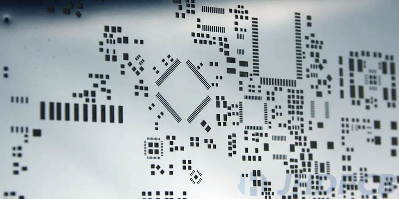
PCB Stencil: Solder paste stencil for PCB assembly.
directory What is PCB stencil? The Advantages of SMD PCB Stencil. What are the types of PCB stencil?
PCB Gerber Files: Ultimate Guide for Beginners.
directory What is a Gerber file? How Gerber Files Are Used In PCB Manufacturing? What should the Gerber
The Ultimate Guide to UL 94V-0 Circuit Boards
directory What does 94v-0 mean? Material properties for UL94v. What is a 94V-0 circuit board? What is UL
Wave and Reflow Soldering in PCB Soldering: Process Guide
directory What is wave soldering? How to do wave soldering? What is reflow soldering? How to do reflow
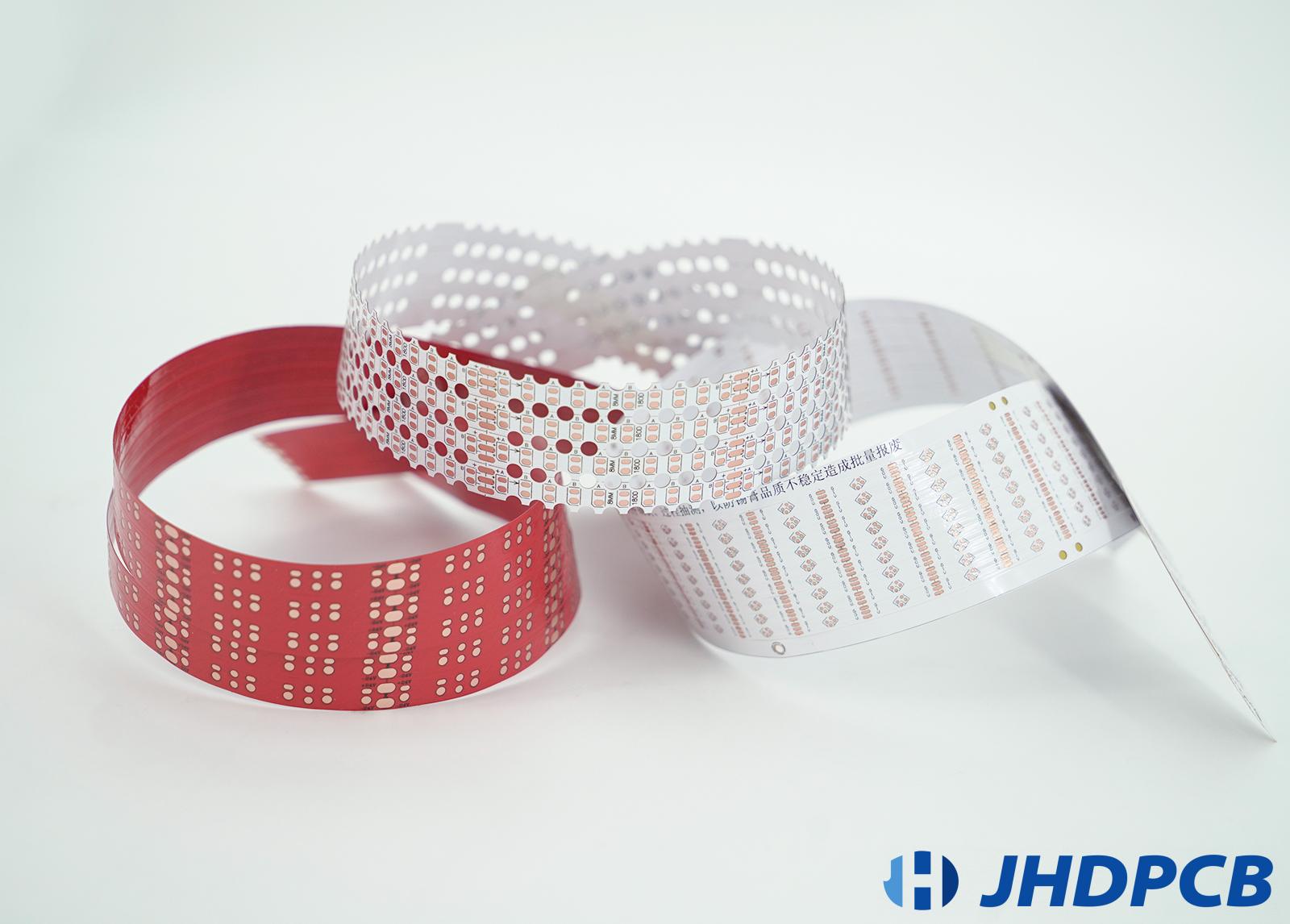
A must-know guide for flex PCB design prerequisites.
directory What are the materials used to make flexible PCBs? Basic structure of the flexible PCBs. Bendability of
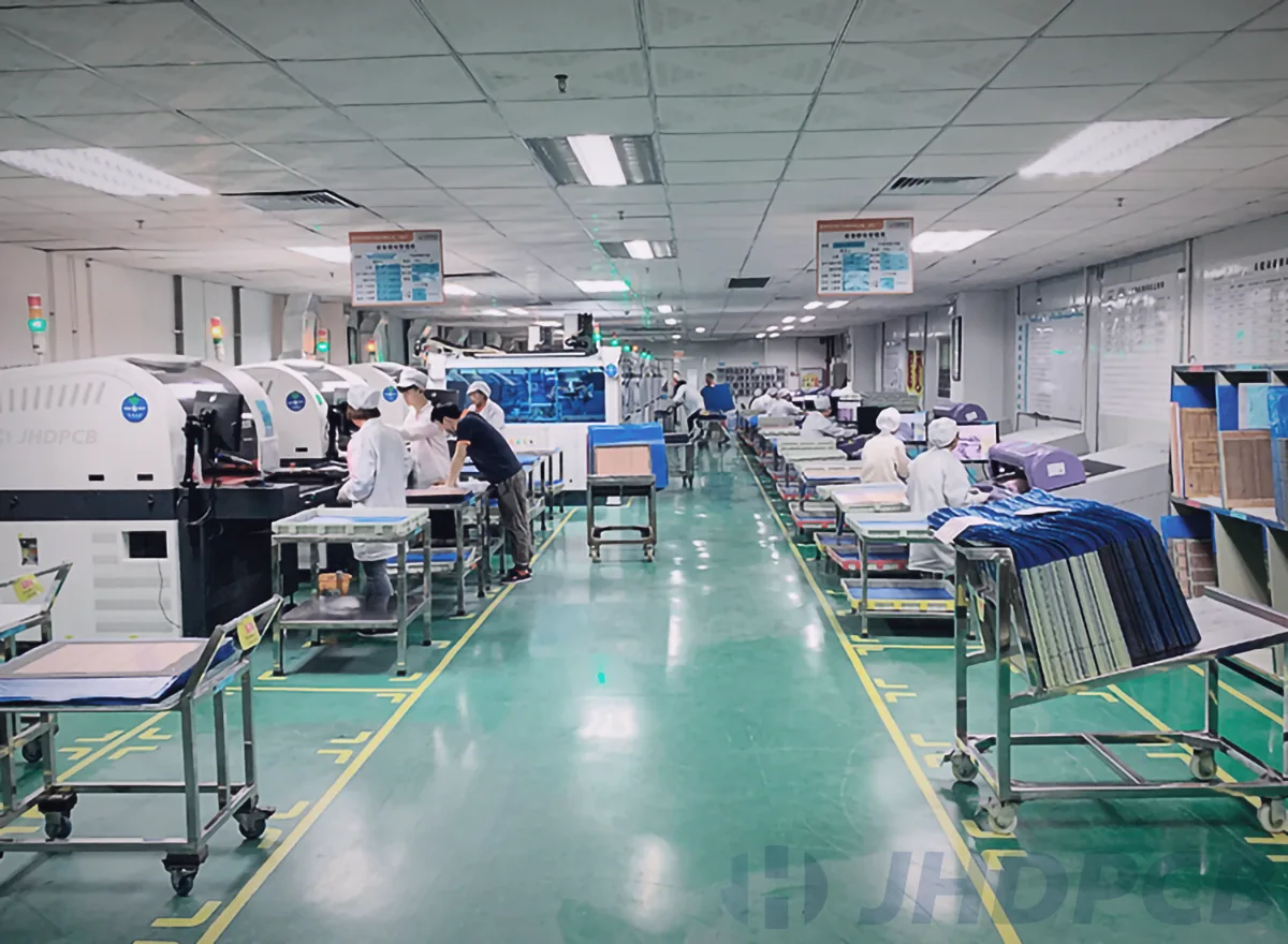
Automatic Optical Inspection (AOI) Guidelines in PCB Manufacturing
directory What is automatic optical inspection? Importance of automated optical inspection test. Features of automatic optical inspection. How
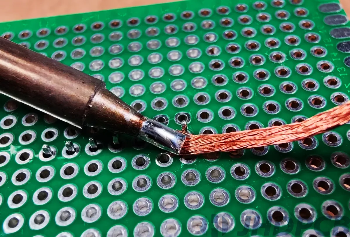
The Ultimate Guide to PCB Solder Wick and Wicking.
directory What is a solder wick? Characteristics of solder wicks. How to choose the correct desoldering wick? How
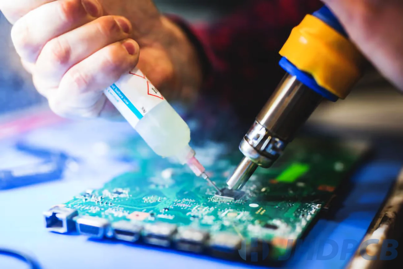
Soldering Flux in PCB Production: The Ultimate Guide to Roles and Types.
directory What is a soldering flux? What is soldering flux paste? What is the role of flux in
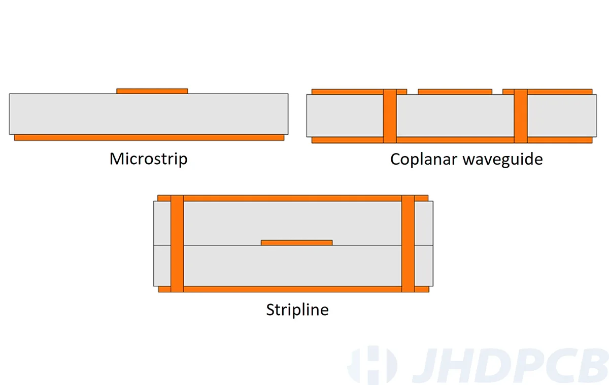
Ultimate Guide to Microstrip, Stripline and CPW in PCBs
directory What is microstrip in PCB? Factors and formulas for microstrip design. What are the impedance control factors


