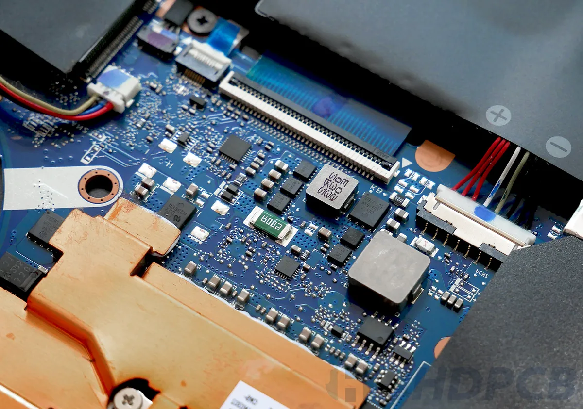
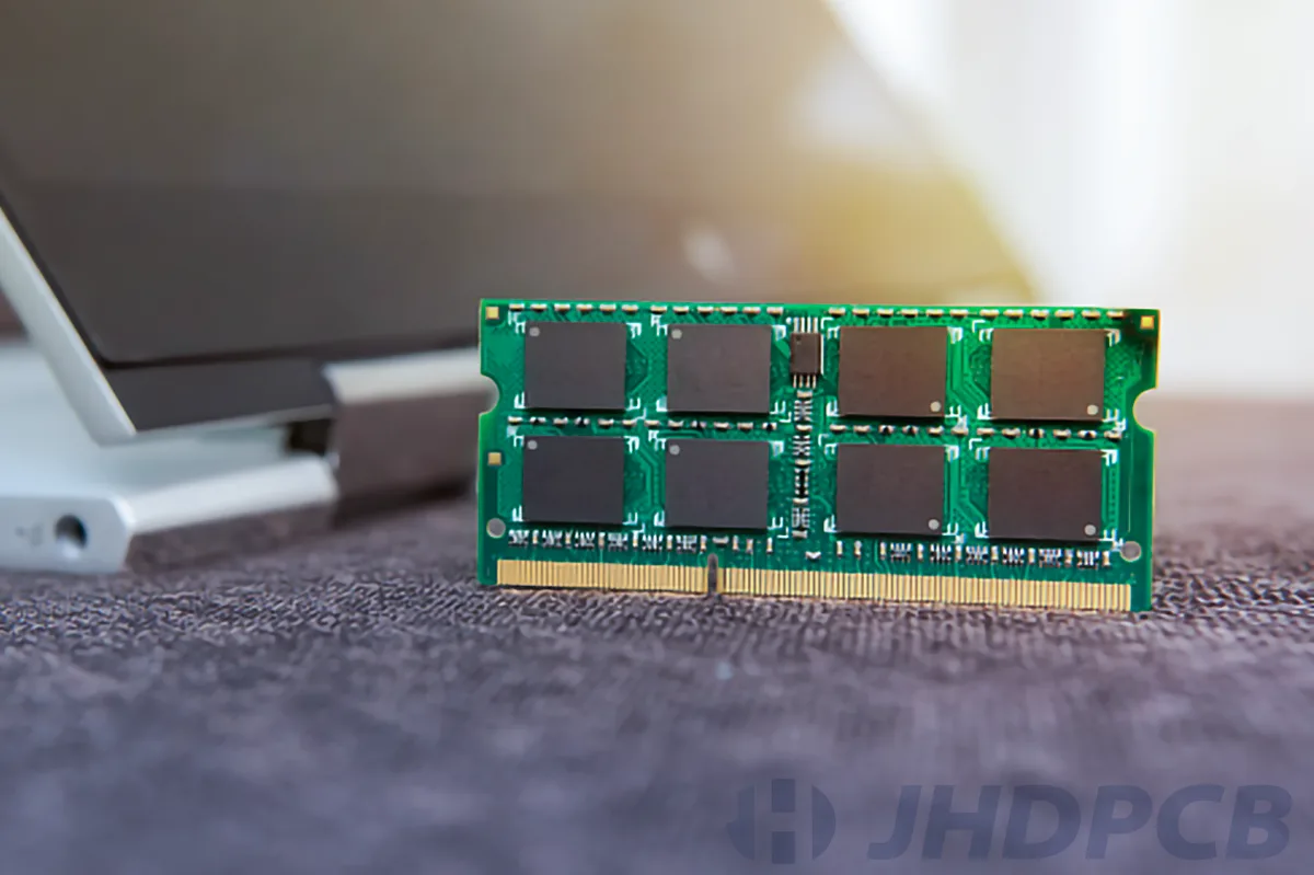
Fully understand PCB components: parts, codes and functions.
directory What are circuit board components? What are the common electronic components on PCB? Common PCB components codes.
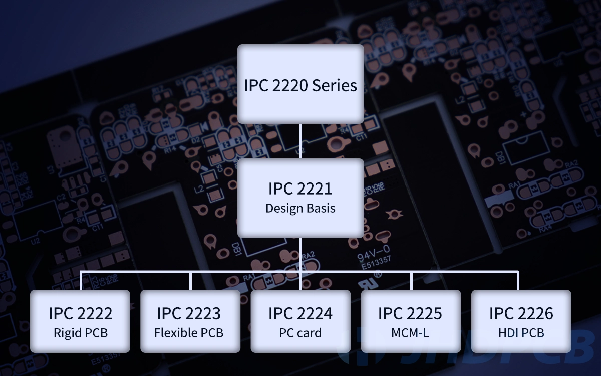
Applying the IPC 2221 standard to printed circuit board design.
directory What is ipc-2221 standard? What functions does IPC-2221 do? What clearance standards does IPC-2221 define for production?
IPC Class Standards for PCB Manufacturing: Rule Definitions.
directory What is IPC? Why implement IPC standards? What IPC standards are there for the PCB production process?
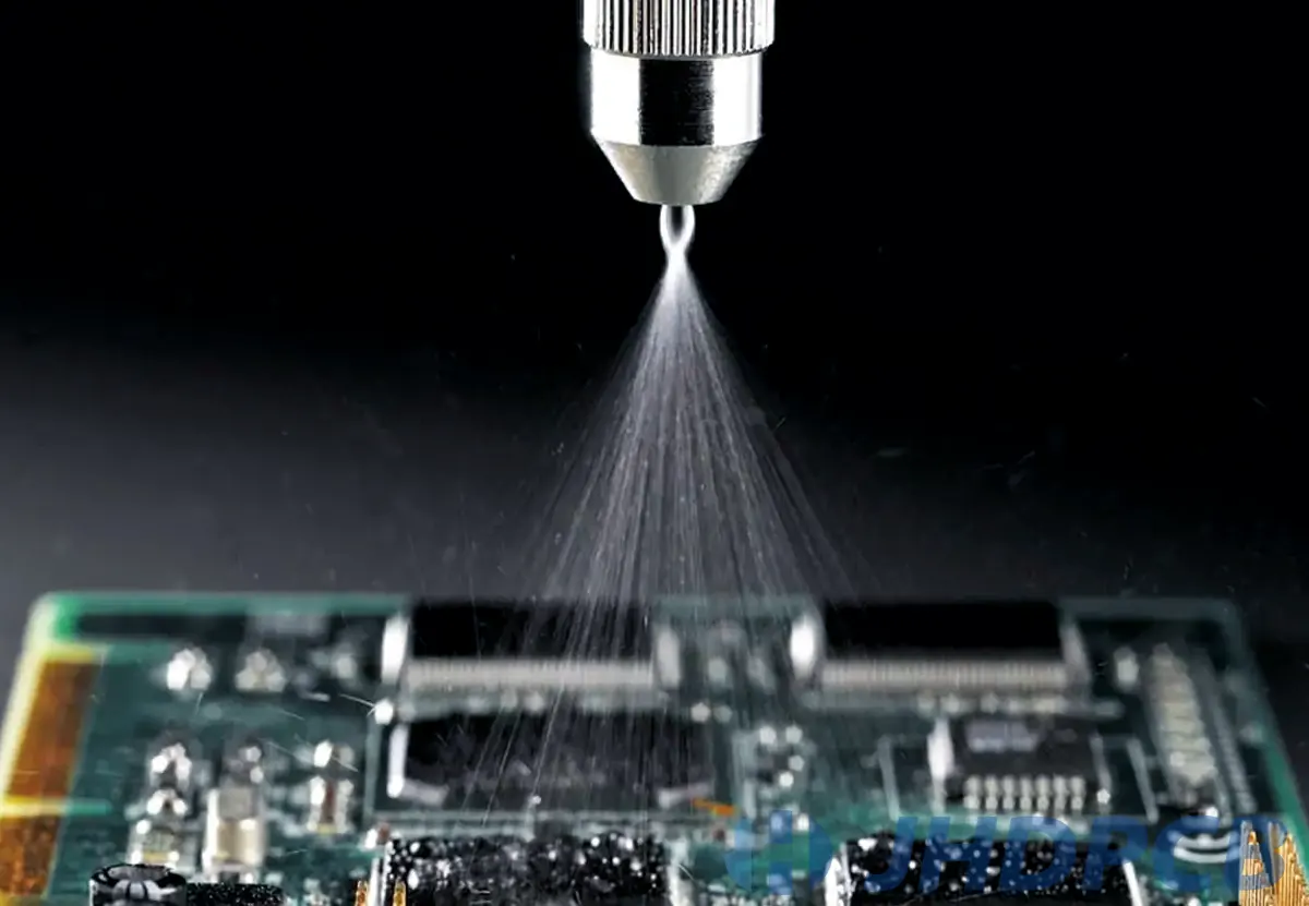
Conformal Coatings: Guidelines for Application Methods, Measurement Tests, and More.
directory What is a conformal coating? Are Conformal Coatings Conductive? How does conformal coating help PCBs? What chemical
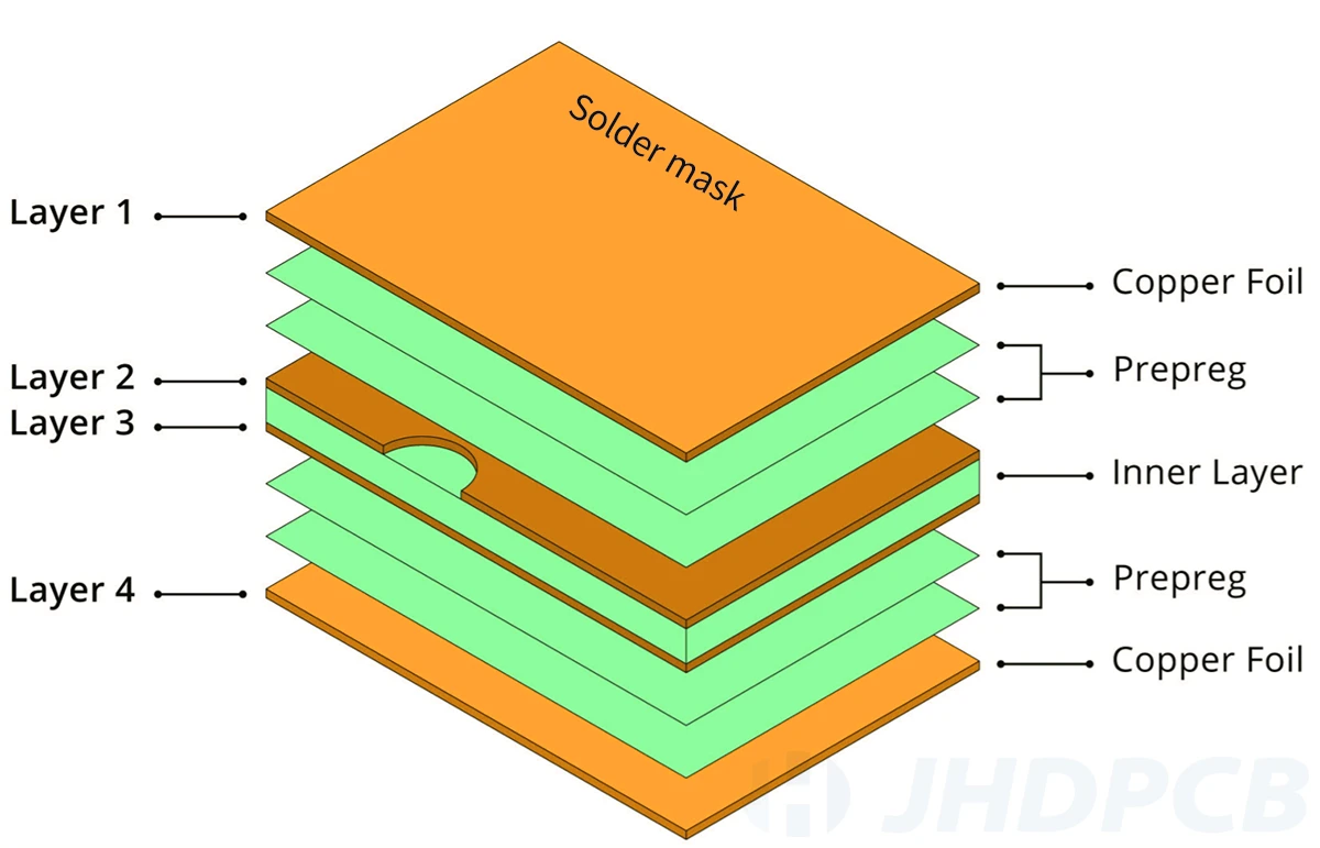
Ultimate Guide to PCB Prepregs: VS core VS laminate.
directory What is prepreg in PCB? Characteristics of prepregs. How is the pregreg made? The Differences Between PCB
PWB VS PCB: Differences and In-Depth Guide.
directory What is PWB? What is a PCB? What is the difference between PWB vs PCB? What other
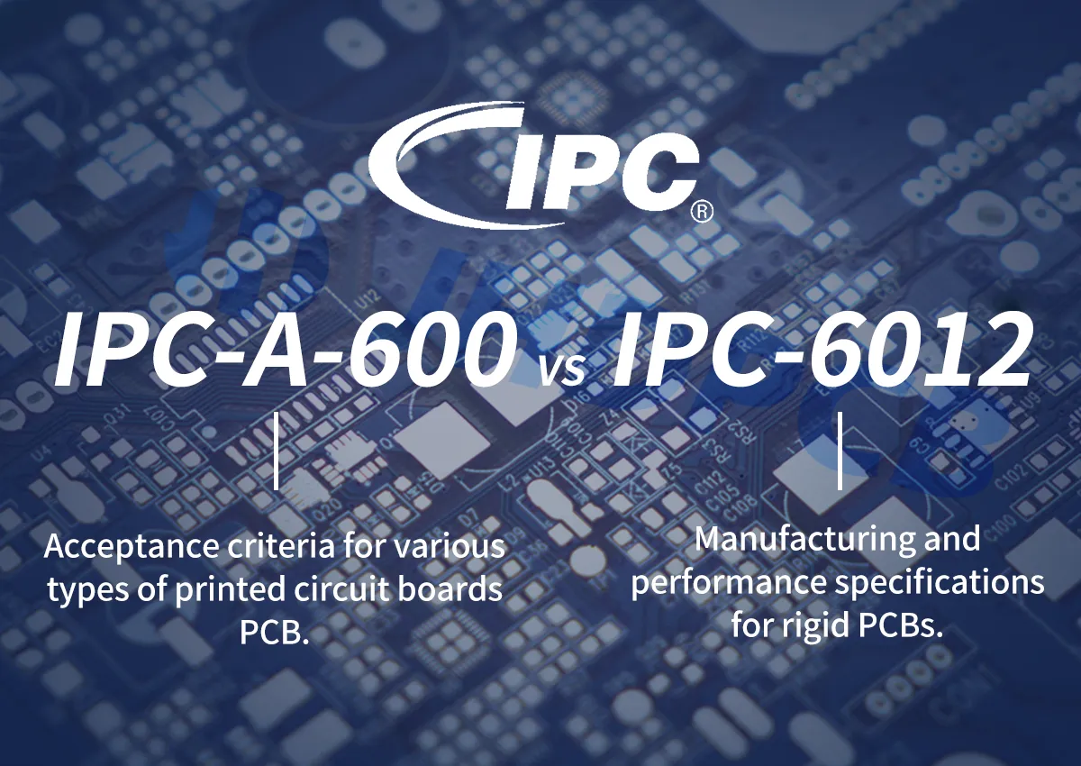
The role of IPC A 600 and IPC 6012 standards in PCB manufacturing
directory What is IPC? What is the IPC-A-600 standard? What is the IPC-6012 standard? What does IPC-6012 regulate
In-depth guide to PCB annular ring manufacturing
directory What is annular ring in pcb? The importance of PCB annular ring size. How to calculate annular
Chip Scale Package: A Guide to CSP Package Forms and Types
directory What is CSP chip scale package? Features of Chip Scale Packaging. What are the common forms of


