
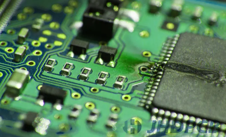
For the hobbyist, knowing how PCBs function and how to fix them is essential if you want to learn how to maintain your own systems and projects. Once you have learnt this techinical ability, you will find that it stimulates your interest and opportunities to gradually explore simple to complex related electronics repairs. This is the first step makes toward more superior electronics restore work.
For professional electrical engineers, mastering the skill of repair circuit board is a matter of course. Electrical engineers should feel confident in their PCB skills as they are more motivated to pursue knowledge of this elementary skill. Today, many commercial fields as well as individual users are increasingly relying on more complex electronic products, and most of them need PCBs. Only by fully understanding how to diagnose, repair or replace circuit board failures, can electrical engineers perform troubleshooting on various electronic devices with ease.
Obviously, the main benefit of repairing a PCB is that it restores the functionality of the electronic products to its primary standards. Besides, repairing a PCB can be generally done quicker than replacing it, depending on the extent of the damage. Beyond that, it’s important to note that repairs are usually less expensive.
In the end, both amateurs and professional electrical engineers have good reasons to get involved in learning about PCB circuit board repairs. A person who is passionate about researching and practicing the recycling or upcycling of electronic products, or maximizing the lifespan of electronic equipment, he will surely gain a great deal of accomplishment in the process of repairing PCBs, identifying and replacing faulty circuit board components, etc.
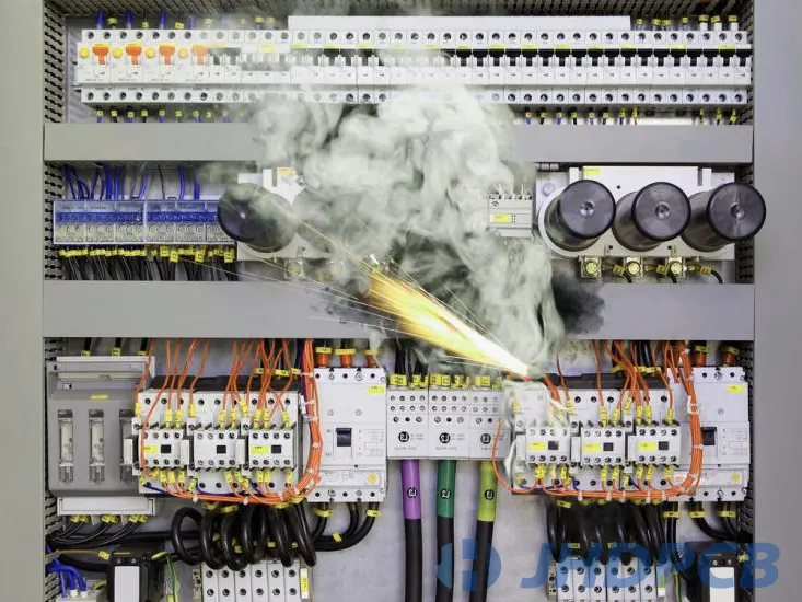
Before doing any curcuit board repairs, we need to inspect and understand why it failed. Familiarity with some of the common causes of circuit board failure is essential. If something goes wrong with your electronics, you can find out why it failed. You can know where to start to successfully solve problems.
The followings are the common causes of PCB circuit board failure:
- Physical Damage.
Generally speaking, when a PCB fails, it is usually because of physical damage to the electronic device or the components within it. Causes of physical damage generally relate to physical shock or pressure. However, in rare cases, it might be because the device has fallen from a high place, or has experienced a violent crash. Sometimes the electronic device is manually disassembled and the circuit board is damaged. - Defective PCB Assembly.
The second most common cause is PCB assembly failure. If the PCB is not physically damaged by impact, you can consider that the PCB failure is related to the components of the circuit board. The damaged component can be anything from a capacitor to a diode or a microprocessor, most are diodes, transistors or ICs. Over time, components are discontinued or failed. If it is determined that the PCB failure is caused by a component, we need to repair or replace it in time. - Trace Damage.
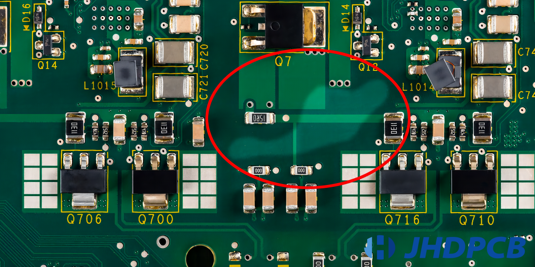
We know that traces on a circuit board are conductive paths made of copper or silver. Many times we can see trace problems with the naked eye, but sometimes we can’t. If the traces are damaged, the board will not operate or function. Some usual reasons of trace damage consider metal dust contamination, overheating and normal wear and tear, lightning strikes, severe power surges or short circuits, etc. - Poor Design.
From the design of the PCB board to the assembly of all links, different responsible persons will participate. Although today’s electrical engineers are excellent, human subjective errors may occur in the production process of PCBs. This can result in poor design of the board, which can lead to failure of the PCB. However, these errors are not intented. Human errors are generally misinterpretation of design drawings and installation errors of electronic components. What’s more, when soldering electronic elements, there may be lead to leakage of welding. - Environmental Factors.
PCB circuit boards have certain requirements on the environment. Excessive heat or humidity can cause some materials in the PCB to expand. In addition, exposure to air, water, chemicals, or other contaminants may cause rust to form on metal conductors. This increases the possibility of short circuits and reduces the efficiency of the board. Dust, fibers, hair and even insects that are ubiquitous in life will sneak into PCBs during the manufacturing process. - Static Electricity Damage.
Through the investigation, it was found that component defects may occur during the PCB assembly process. The main cause of this problem is static electricity. Because the PCB will react when it comes into contact with static electricity, even a small amount of static electricity may damage the PCB. - High Temperature Damage.
One situation is that the distance between the various electronic components in the circuit board is too close. Then when the PCB board is running, high temperature will be generated between the components. This can lead to burnout of electronic components.
Another situation is that when the PCB board is in a high temperature environment (above 170 degrees), it will cause the PCB components to burn out. Usually under high temperature application conditions we suggest to use thick copper PCB to help better heat dissipation, or use high TG PCB to help solve the problem. This is a very serious failure. , sometimes the circuit board needs to be replaced completely.
When servicing printed circuit boards (PCBs), we follow some precautions to prevent further damage. Here are some Necessary safety measures:
- Wear safe explosion-proof glasses:
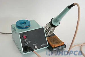
When doing PCB repairs, it is inevitable that solder will splatter. Especially when the soldering iron melts the tin wire, some liquid will be splashed. Therefore, wearing safety glasses can isolate your eyes from dangerous objects, they play a protective role. - Discharge theElectronics:
When we are ready to repair damaged electronic equipment, be sure to unplug the electronic equipment and ensure that the PCB board is completely discharged. In particular, we should pay attention to the power supply and capacitor can be charged, to ensure that they are safely discharged. At the same time we remove the extra supplementary battery. Why do we do this? First, the purpose of this is to prevent short circuits in the electronics. The second reason is to protect our own safety from electrocution. - Wear an Antistatic Wrist Strap:
Electrostatic discharge(ESD) is the sudden flow of sparks across two surfaces. There is a current difference between these two surfaces. In order to maintain balance, the one with more current will flow to the one with less current, thus generating static electricity. Anti-static wrist straps have a conductive surface that dissipates the skin and thus is able to dissipate excess charges. In addition, when repairing the PCB, you should also wear anti-static hats, overalls and shoes to ensure your own safety. - Reduce Environmental Pollution:
Before PCB maintenance, we need clean our hands, use electronic safety hand sanitizer and clean the edges of PCB to ensure the smooth progress of the maintenance process. The reason for this is that the attachments on the hands and the edge of the PCB, such as water and salt, may cause corrosion and short circuit of the PCB board. Therefore, during PCB repairing, we must be sure to use electronic safety hand sanitizer to clean hands and prevent more failures on the circuit board. Wear work gloves for better protection.
Specific steps for circuit board repairing
Before starting the repair, you need to gather the PCB repair kits and materials needed to repair the PCB. For general repairs, you will need:
Sharp knife or flathead, screwdriver or sandpaper, Welding gun, Adhesive copper tape, Scissors or craft knife, Hot air gun, Tweezers, Paper clip, Pen, Cotton swabs and rubbing alcohol.
With all the tools at hand, then follow our PCB rework and repair guide:
| Step | Operate |
|---|---|
| Step 1-Remove the damaged components or pads | First, to prevent the PCB from moving while you work, you can first fix the board on the workbench with tape. If the PCB pads have been damaged, we need to do PCB pad repair with a sharp knife or flathead screwdriver to remove the component. |
| Step 2-Clean tracks and remove solder | After repairing the PCB, use some tools to remove the solder from the tracks. Such as scissors, sharp knife, sandpaper and cotton swab dipped in alcohol, etc. Whichever material you use, make sure the track is clean and bare. |
| Step 3-Put the copper tape on the track | After the track is cleaned, place the adhesive copper tape on top of the track and make sure the copper tape is flush with the track. At the same time, part of the current flow in the existing vias and surrounding areas is to be covered. This will provide a good connection to the pad or new component. |
| Step 4-Welded joints | With the copper tape PCB repair in place, it’s time to solder the new copper tape to the joints where the existing track connections on the repaired PCB are made. You need to pay attention during this process: make sure you can complete this process in once. Because the copper strip melts quickly at welding temperatures, act quickly and apply as little heat as possible. |
| Step 5-Recovery the PCB vias | Use a hard material with a round tip like a pen. Press and rub where you just soldered to ensure that the copper tape sticks firmly to the pad area. The adhesive remains tacky after heat is applied to the pad area. After you determine where the through-holes are, you can use paper clips or other similar tools to pierce. |
| Step 6-Place and solder your components | After completing the above steps, you should now place the new component onto the PCB and solder it. Plug the lead wire of the new part into the through hole first, then overturn the PCB. The next step is to apply solder to the pads and heat until the solder melts. Then hold the leads in place until the solder cools down. The operation of the other pad is the same as above. What you need to pay attention to is minimizing the heating time to ensure that the welding goes smoothly. |
| Step 7-Trim excess tape from repaired area | Once the new component is in place, you’ll need to use a craft knife or a pair of scissor to cut away any excess copper tape in the repair area. Your steps above may fix the PCB. But the tracks, pads, and joint won’t be as structurally perfect as the primary PCB board. Regardless, you’ve given new life and meaning to something that so many people throw away as trash. |
How to repair printed circuit board soldering errors?
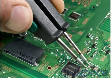
Soldering is a relatively simple concept, the process of connecting two metals of different types by melting solder. If there is a soldering problem, the usual solution is to remove and replace the faulty component, sometimes by stripping off the excess solder. Here are some common desoldering methods:
| Method | Detailed |
|---|---|
| Solder wicking
| Solder wick, wick, solder braid, and desoldering wick are all names refer to the same thing. It refers to a pre-fluxed copper braid used for solder removal. It removes excess solder and corrects solder bridging in isolated areas without affecting the entire board or nearby components. Because desoldering wick only removes uncovered solder, you’ll need to remove the component covering the contact area before starting this operation. |
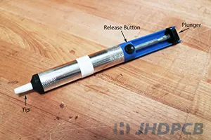
| Desoldering sucker
| This is one of the best ways to desolder components. It works by using a spring-loaded vacuum to draw the solder upwards while it is heated. Note that desoldering suckers can only pick up less solder at a time, so it will take you several operations to move the component. Because it only removes uncovered solder, so the components covering the contact area must be removed before operation. |
| Desoldering station
| A desoldering station works well for desoldering. This device has a soldering iron tip with a small hole in the middle. It will draw up the solder as it melts. But the desoldering station can only remove the uncovered solder, so the components covering the contact area need to be removed before proceeding. |
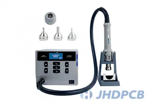
| Hot air welding station
| A hot air welding station is a useful desoldering tool. It works by the hot air coming out of the hot air solder station to melt the solder in the repaired area. After this, you can use a vacuum lifter or tweezers to remove the component. It should be noted that the heating time cannot be too long, otherwise the copper plating on the PCB will melt and damage the circuit board. |
| Hot tweezers
| The material of the hot tweezers is a soldering iron. With thermal tweezers clamped over the lead area, the tip of the tweezers heats up and transfers heat directly to the component, then melting the solder. Hot tweezers melt the target component more accurately than other tools. Damage to nearby components is avoided. |
| Hot plate
| The hot plate can melt all the solder joints at the same time, you just need to put the PCB on it. Its benefit is that multiple components can be removed at once. The disadvantage is that because of its large melting range, it may cause damage to the entire circuit board or other good components. |
How to repair PCB pads?
| Step | Detailed |
|---|---|
Tidy Up the Impaired Track 1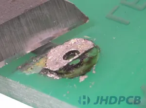 | Remove as little of the impaired part as possible in order to restore the track. In order to avoid unnecessary damage during disassembly, it is recommended to use a sharp knife for removal. |
Tidy Up the Impaired Track 2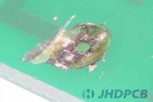 | It should look like the picture after the impaired track is removed. |
Expose the Track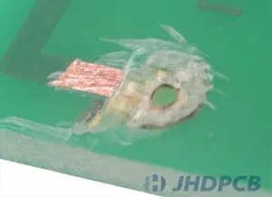 | To make the tape stick even more firmly, take any residual burnt substance away from the PCB. Or you can use fine-grit sandpaper, a sharp screwdriver, or a knife to scrape off slight solder resist. Make sure the uncovered track is shiny and clean. |
Stick Copper Tape to Uncovered Track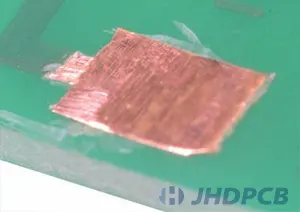 | Apply copper tape to the track, making sure that the copper tape overlaps the track slightly. |
Solder Copper Tape Joints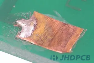 | Weld the joint being repaired. Note that you need to do this quickly as the copper tape adhesive may melt due to the heat while soldering. Adhesives generally stay tacky as the tape cools. |
Pierce a Hole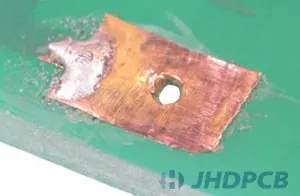 | Rub the pad area with a round and hard object like the non-writing end of a ballpoint pen. This action will force the copper tape down and over the pad area. Then the pad hole will reveal, which you can pierce with a paper clip, component lead, or similar items. |
Solder in the component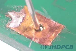 | Once you’ve done the above, you can start installing and soldering components. In this process, it is necessary to avoid excessive welding time as much as possible, so as to prevent the adhesive from melting and suspending the maintenance. |
Carefully Trim the Restoration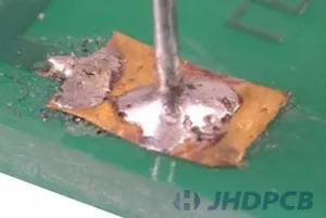 | Next you can cut the copper tape carefully. Trim the copper tape to a certain length using a utility knife or scissors. After this, you can also trim the excess tape. Because the repaired section is more fragile than the previous track, use caution when trimming the tape. |
How to find a short on a circuit board?
During the PCB design process, electrical engineers may face the damage to circuit board. Short circuits are one of the most destructive and troublesome damages to a PCB. To know how to find shorts on PCBs, you need to understand these three main points:
The signs of shorts-
Signs of a short circuit can appear as a variety of symptoms, from obvious visual damage to subtle damage that is only discovered during testing. The simple case is that when applying power to the PCB, the indication of a short circuit may be that you will see some arcing or hear a “pop”. If this happens, you can easily spot where the short is.
Some subtle shorts can occur between input pins or other components. These conditions are only discovered when the functionality of the circuit is tested. Although the stability of the PCB is guaranteed in most cases, it is still important to run the test.
Methods to find shorts on PCBs-
When you master some necessary electronic theory, tools for locating short circuits, and keen eyes, you will be able to locate the location of the short circuit when it occurs in the circuit. Regardless of which of the following tests are performed, ensure a thorough visual inspection of the PCB.
- Visual Test.
Vision aids and magnifying glasses can help you spot some obvious shorts. Examples include incompletely etched copper areas, or solder joints between pins. - Find the Location of the Burnt Components.
If a short circuit occurs, it may cause scorching or burn marks. You can easily locate this problem because of the contrast between the green of the PCB board and the burnt brown. - Use a Digital Multimeter.
A digital multimeter can help you find the approximate physical location of the short, giving you a better idea of where to start looking. Start with the power supply and test each pair of near traces and pads one by one. - Use Thermal Camera.
Although the budget is a bit high for a thermal camera, it will be of great help in locating short circuits. A short circuit can cause a lot of current to flow out and generate heat. A thermal camera can help you pinpoint areas of high heat. Then perform visual verification. - Destructive Testing.
If none of the above works, you can test the board for shorts by destructive testing. You can physically disassemble the board or cut some traces to locate the short. This method is also beneficial for you to understand whether the short circuit fault is a manufacturing or design deficiency.
Causes of short on PCB-
1) The PCB short circuit problem may be caused by improper design or manufacture. Inconsistent weld pad design is the main cause of PCB short circuit. We can replace the commonly used circular pads with oval pads to avoid short circuits, increase the distance between points. During the manufacturing process, if a thin copper line is left in the PCB board, it is very likely to cause a short circuit of the thin line.
2) Sometimes, short circuit occurs on electronic components. Generally speaking, we only need to remove the problematic components to restore it. But sometimes the short circuit may be caused by the reverse direction of the PCB electronic components. So carefully check the orientation of the components when investigating the cause of the short.
3) The third reason for the short circuit is the automatic plug-in problem, that is, crooked feet. We should ensure that the distance between the circuit and the solder joint does not exceed 2mm. Too long a distance can cause electronics to come off, which in turn can cause a short circuit. Click to view detailed through-hole plug-in assembly process information.
In addition, PCB short circuits can also be caused by other reasons. For instance: solder mask failure, too large substrate hole, board surface contamination, low tin furnace temperature, poor solderability of the board, etc.
How to repair PCB trace?
PCB trace is highly conductive track that join the microchips and other vital components on a PCB board. Traces on a PCB can suffer damage in different ways. Mostly, the cause of trace failures is corrosion. May be caused by improper storage. Or the battery or electrolytic capacitor has leaks, then causing corrosion and cause traces failures.
PCB track repair steps:
- Find the faulty trace, and distinguish the joints and pads on each extremity.
- Using a cleaning cloth dampened with rubbing alcohol, wipe off grease and dirt. until the copper color is clearly visible.
- Cut off any loose trace Please operate this step carefully to avoid damage to other components on the PCB.
- Check whether there is enough visible traceat the lifting end. If present, weld a wire jumper from that location to the other end of a connection pad or joint or trace. If it does not exist, it needs to be welded from one joint or connection pad to another joint or connection pad to achieve the effect of completely replacing the trace path.
How to repair holes in PCB?
Vias or through holes damage can occur when improperly removing through-hole devices or performing repairs to PCB boards. The following is the procedure for PCB through hole repair/PCB eyelet repair. Before that, you need to prepare the following PCB repair tools:
Flux, Calipers (or drill guage template), Knife, Wet wipes, Hammer, Microscope, Eyelet kit, Eyelet forming tool, Drill, Drill bits or ball mill, Cleaning solvent, Weld, Welding iron.
| Step | Detailed |
|---|---|
| Find the Proper Drill Bit Size | Try drill sizes in order from small to large until you find one that can be slightly larger than the plated hole opening. In order to drill the plating hole smoothly. |
| Drill the Hole | Drill the hole with a hand drill and ensure you drill perpendicular to the plane of the PCB. |
| Use a Drill Template Gauge to Determine Eyelet OD | Use the drill template gauge to find the correct size of the hole’s outside diameter. |
| Verify that the Eyelet Size is Correct | Use a drill gauge to ensure the correct eyelet size. |
| Roll the Eyelet Flange Using a Swage Tool and Hammer | Place the flange side of the eyelet on the swage tool. Ensure the circuit board is level. Use a pick of 90 degree to evenly “roll” out the flange. The hammer for a flat setting. |
| Connect Trace to the Eyelet | Add liquid flux and weld the pads to the substitution eyelet to make an electrical connection. Make sure the solder “wicks” up to 75% of the sides of the flange. |
| Electrical Inspection and Testing | Conduct an electrical test to ensure connections are in place. |
How to repair PCB gold finger?
Gold fingers are gold-plated posts located on the connective edge of a PCB board. Because the gold finger is located in the edge area, it is prone to failure. Sometimes solder spatter occurs during soldering.
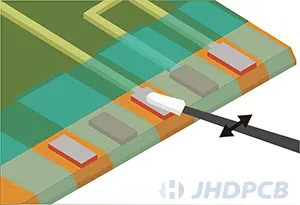
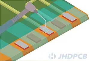
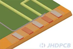
| Goldfinger Common Faults | Image display |
|---|---|
| Scratched and Worn Gold Fingers | 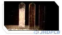 |
| Gold finger with Solder | 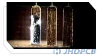 |
| Contaminated Goldfinger | 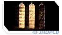 |
When an edge contact is scratched, torn, contaminated or damaged, there are steps we take to repair or replace the contacts. Restores faulty contacts to complete functional durability and conductivity.
| Step | Detailed Operation |
|---|---|
| Clean and inspect the areas that need re-plating. Depending on the degree of spatter or damage on the gold-plated surface, consider whether a re-plating process is required. |
| Clean up residual solder. Apply tape on and near the area where the solder splattered, then use the solution to remove the residual solder on the surface. See if the pad needs to be replaced, and if so replace it with a new gold-plated pad. |
| Rinse off the solution residue on the PCB, then dry the board and inspect it. |
| Attach a bus in the immediate vicinity of the re-plating area. Using a small power supply with a cotton swab attached to the electrodes, the electroplating process is carried out with nickel and gold plating solutions when necessary. Inspect and test the area after plating is complete. |