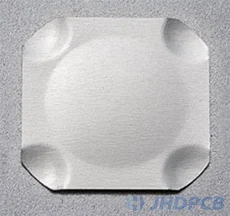
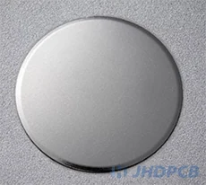
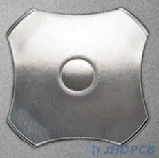
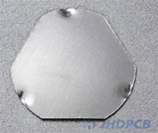
What is the solder pad in PCB design and production?
jhdpcb@gmail.com
What is a PCB solder pad?
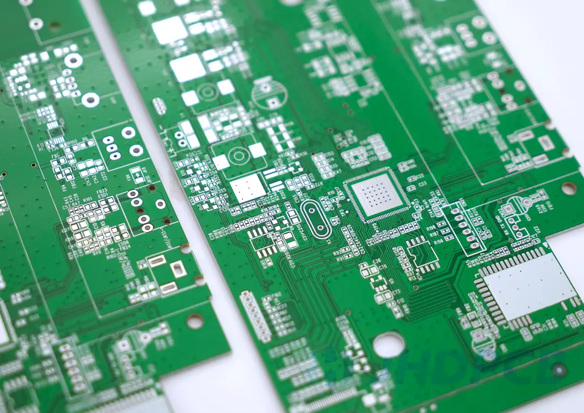
What is a solder pad? It is a specific area that you can see on the PCB of an integrated circuit. It is a small area of copper on the PCB that allows certain components to be soldered to the PCB. PCB solder pad is placed where component pins are soldered and held mechanically like a piece of copper. There are two types of pads: surface mount pads and through-hole pads. These pads pcb are connected to the traces on the board to form a circuit. In some cases, they also improve heat dissipation on the PCB.
What are some common PCB pad types?
The process type of the PCB pad.
The process of pads is generally divided into two types: pads for surface mounting and pads for through-hole mounting.
Pads for surface mount.
Pads for component mounting are referred to as surface mount pads. These pads have the following characteristics.
- pads that have a surface made of copper. They can be rectangular, round, square or oblong.
- Solder mask layer;
- Solder paste;
- Number of pads (number of pads present on the part).
A correct pad layout is important to ensure the manufacturability of the BGA factor. In this regard, there are basically two types of BGA pads. There are pads of non-solder masks pads (NSMD) and pads with solder masks pads (SMD).
Non-solder mask defined BGA pads (NSMD):
Non-solder mask defined pads differ from pads defined with solder mask (SMD pads) because the solder mask must not contact the copper area. Alternatively, the mask is made so that there is a disconnect between the adjacent pad and the solder mask.
NSMD pads can be smaller than the solder ball diameter, with the pad size reduction being 20% of the ball diameter. This results in a greater number of adjacent pads, which facilitates decode routing, and is used for high-concentration, well-beveled BGA chips. A disadvantage of NSMD pads is that they are prone to delamination due to thermal and mechanical stress. However, delamination of NSMD pads can be avoided if standardized chips are used in design and handling.
Solder mask defined (SMD) BGA Pads:
SMD pads can be identified by the solder mask openings placed on the BGA pads; SMD pads have solder mask holes, which are larger than the diameter of the pad addressed by the mask initiator. This is done to reduce the size of the copper pad to which the component is soldered.
The prototype shows how the solder mask is mounted to cover the component on the copper pad pcb below. This provides two advantages. First, the stabilizing mask prevents the pads from detaching from the PCB due to mechanical or thermal stress. Second, the mask’s masking path creates an environment in which each BGA pad is aligned as the component moves through the soldering process.
The copper layer of the SMD BGA pad has traditionally had a rounded area corresponding to the BGA pad; to form the SMD cladding, a reduction of 20% has traditionally been made.
Through-hole pads.
Mounting pads for components with through holes are called through-hole pads and are available in two types.
The plated Through-holes (PTH):
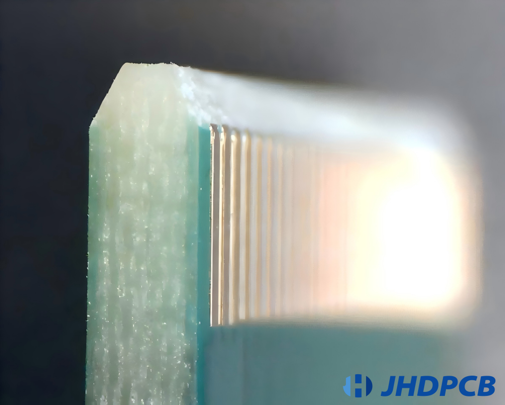
PTH is a plated through-hole. The walls of the hole are bronzed, sometimes with a weld or other protective coating. The coating of the holes is done by the process of electrolysis. This coating allows the creation of electrical connections between the different layers of the plate. In encapsulated substrates, the holes are drilled on the edges of the substrate. These half-holes are metalized to make connections to different subunits.
Non-plated through-holes (NPTH):
NPTH refers to a pad that is not laminated into the hole. This pad is mainly used in single-sided PCBs, or these holes are used to secure the PCB in the package, and screws are inserted through these holes. Traditionally, unplated holes have a free copper area around the hole (similar to the edge opening of a PCB), which prevents short circuits between the copper layer and the component being mounted.
Each section of a plated-through pad is commonly referred to as a pad stack and consists of.
1. upper pad;
2. lower pad;
3. inner pad;
4. holes;
5. annular ring;
6. pin number.
Common shapes of PCB pads.
PCB solder pads are designed in various shapes to suit different application fields. In the following, JHDPCB lists some of our commonly used shape layouts. Regardless of the desired shape, including single-sided, double-sided contact pads, and a variety of customized pads. JHDPCB production and customer service teams are happy to provide you with high-quality services.
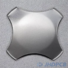
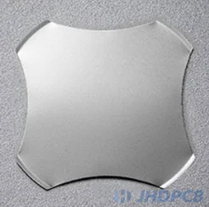
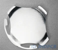
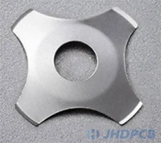
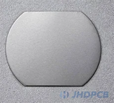
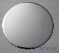
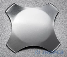
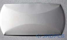
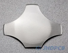
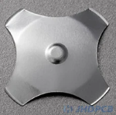
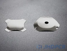
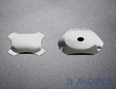
Metal domes are usually placed on a gold or tin contact plate, and each JHD metal dome has a corresponding PCB contact pad. Below are the single-sided and double-sided contact pads, broken down by metal dome series. If you need design help or have any other questions, please feel free to contact us directly.
| Contact pads by dome series | |||
|---|---|---|---|
| Series name | Legend display | Series name | Legend display |
| F-SERIES |
| GX-SERIES |
|
| S-SERIES |
| SQ-SERIES |
|
| M-SERIES |
| RCG-SERIES |
|
| WT-SERIES |
| BL-SERIES |
|
| RK-SERIES |
| P-SERIES |
|
| U-SERIES |
| E-SERIES |
|
| DT-SERIES |
| TC-SERIES |
|
| FB-SERIES |
| TB-SERIES |
|
| Special-shaped customized pad series | ||
|---|---|---|
| Shape type | Introduction | Example diagram |
| Single sided | (Suitable for F, U, TC, SQ, GX, and RCG Series domes) The single-sided PCB pad is ideal for four-sided domes and also does not affect the track when the dome is activated. | 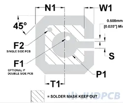 |
| Double sided | (Suitable for all domes except oblong) Double sided PCB pads are available for all dome styles except elongated and dual action (DT-Series) | 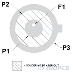 |
| Solder dome | Solder dome is suitable for the single-sided PCB pads ,also known as the S-Series. | 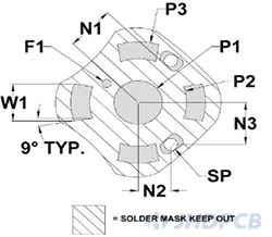 |
| Single sided 3-leg | (Suitable for WT-and E-TDF Series) 0.38mmSingle sided PCB pads can usually be used with three-leg domes, which included the WT-Series and E-TDF-Series. | 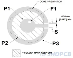 |
| Single sided with center led | (Suitable for BL-Series Domes) Single- sided PCB pads can be used with BL-Series domes with center hole for led. | 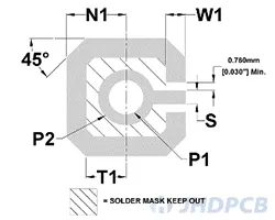 |
| Double sided with center led | Double sided PCB pads can also be used with BL-series domes with center for led. | 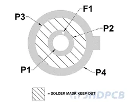 |
| Double sided oblong | (Suitable for RK-Series and E-Series oblong (ONN) domes) | 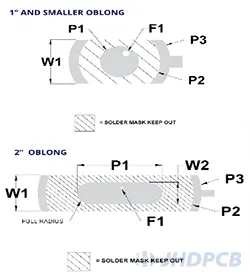 |
| Single& double sided (DT-Series) | (Suitable for DT-Series domes) Single-sided double action contact pads was pads with specifically designed to use with the DT-Series dual action domes. | 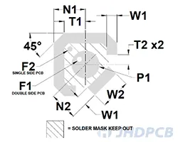 |
| Single& double sided contact pad 4-leg battery | (Suitable for FB-Series domes) Single and double sided contact pad was particularly used to use with the FE-Series battery contacts | 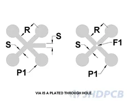 |
| Single& double sided contact pad 3-leg battery | (Suitable for TB-Series domes) Single and double sided pad contact pad was particularly designed to use with the TB-Series battery contacts. | 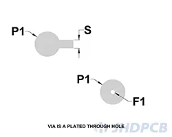 |
The pad stack is represented by a combination of letters and numbers representing different rubber sheet shapes and soil sizes. These combinations are used in conjunction with the terrain drawing conventions defined in the IPC-2220 design standard.
The first section of the pad stack notation contains the landforms written in lowercase. The six basic designations of the landforms are as follows:
- b-oblong;
- c-circular;
- d – D-shaped (square at one end and round at the other);
- r – rectangular;
- s – square;
- u – contour (refers to irregular shapes).
Finally, JHD not only works with conventionally shaped panels such as those mentioned above but can also produce custom-shaped panels to meet design and application requirements.
What factors dictate the size of pads in pcb?
The size of bare PCB pads is influenced by many factors. This section describes some of the factors that determine the size of PCB pads.
- When designing the size of the pads, consideration must be given to component size spacing and tolerances, solder joint size requirements, board accuracy, stability and processability (e.g., placement and positioning accuracy), and the size of the board substrate.
- The size of PCB pads is determined by factors such as component shape and size, board type and quality, assembly equipment capabilities, the type and capabilities of the process used, and the required quality level and standard.
PCB Pads Design Layout Guidelines.
In order for the design of a PCB stack to meet manufacturability and reliability requirements, several factors must be considered.
In this case, this relates to the holes and copper plating of the traces and planner layers.
- Maximum tolerances provide minimum insulation between opposing conductors, which in this case refers to the plating of the holes and copper in the traces and planner layers. Click to view detailed PCB plating knowledge. These must comply with the standards of the intended product. A minimum insulation distance of 4 mm is required for telecommunication equipment and 5 mm for other products.
- Trace to trace connections, through holes and penetrations shall be stable.
- The aspect ratio must be such that the walls of the holes can withstand the stresses of the coating process without failing.
Even if the above guidelines are followed, the drill holes do not always penetrate the panel as intended. This is due to the following factors:
- Movement of the drill bit. Drills may deviate from the desired drill axis (eccentricity).
- Displacement of the film layer.
- Shrinkage of the laminate during the laminating process. This may lead to errors in positioning of drill holes.
- Inaccurate alignment of the layers during lamination.
Misalignment of drill holes means the drill holes are not where they should be. All manufacturers have achieved a tolerance through a process called the drill tolerance. This bore tolerance is used to determine the bore shadow of each borehole. Very accurate manufacturers can reduce the tolerance to ±5 mils, also known as TIR (total included radius). JHDPCB can reduce this tolerance to ±6 mils, and other general manufacturers can reduce it to ±7 mils. It is important for PCB designers to know where PCBs are manufactured so that errors in bore movement can be accurately calculated. It is important for PCB designers to know where PCBs are manufactured so they can accurately calculate errors in drill movement.
Common PCB pad problems during PCB production.
When designing pads for printed circuit boards, the following problems usually arise. These situations must be avoided because they lead to incorrect shapes and sizes of the pads, which leads to undesirable results.
Through-hole breakout:
Through-hole pads need a solid ring to be welded together. The annular ring is the metal between the outer circumference of the plate and the wall of the hole. The ring must be large enough to compensate for the distance of the drill bit from the center of the hole. If the plate is too small, it can split, resulting in broken or incomplete circuits or bad solder.
Insufficient solder joints:
SMT components with solder pads that are too small may not provide an adequate solder strip. In this case, the solder joints of the PCB surface mount process will become weak and damaged.
Floating parts:
In this case, SMT components mounted on oversized pads can move out of position during reflow soldering. This can cause short circuits between the circuits.
Tombstoning parts:
SMT components with two small terminals, such as resistors and capacitors, can cause problems when the pads are not the same size. This defect, in which one pad heats up faster than the other, is called “tombstoning” because the component peels off from the other pad, forming a tombstone-like shape.
Shorts to other metal:
If the solder pad material is smaller than necessary, conductive paths form near the soldered component, which can cause a short circuit. If the pads are larger than necessary, it can affect the wiring between the pads and make wiring more difficult.
Solder bridging:
Solder pads that are too large for surface mount can cause components to float, leading to solder bridging. This occurs when solder is soldered across other network pads or metal elements, causing a direct short circuit. Solder bridges can also occur when the correct characteristics of the solder mask and solder paste are not incorporated into the plate geometry in the CAD tool.
Standards and calculation methods for PCB pad size.
Industry standards for PCB solder pad sizes.
IPC Standards Levels A, B, and C describe different levels of sophistication on a manufacturing scale.
- Density level A is used for general design productivity and is preferred. It is used for low-density boards. In this scenario, the seating geometry is “maximum”. This technique is used to achieve the highest possible performance.
- Density level B is used for medium design productivity and is the standard level, suitable for reflow, wave, drag and dip soldering. In this scenario, the imprinted shape is “medium”. This approach provides reliable brazing conditions.
- Density level C is used for high repeatable designs, is a reduced level and is used for high component densities. In this case, the seating geometry is “minimal”. This approach is used for portable and handheld devices.
Padstack defaults:
- Solder masks are scaled in proportion 1:1 to the mass size.
- Paste masks are scaled in proportion 1:1 to the size of the mass.
- Assembly layer soils are scaled in proportion to the size of the ground 11.
- The inner and outer layer soils have the same shape.
- The dimensions of the primary and secondary soil are the same.
- The shape, holes and mounting holes of the inner layer soil are round.
- The dimensions of the inner diameter, outer diameter and width of the radii of the thermocouple correspond to lPC layers A, B and C. The thermocouple has four radii.
- The dimensions of the ground clearance and spacer correspond to IPC level A B or C.
PTH Hole and Pad Diameter Size Calculation.
1. Determine the maximum diameter of the lead.
The maximum available conductor diameter shall be determined from the component enclosure drawing or data sheet. The following figure shows the maximum lead diameters for different geometries.
– Round PTH conductors require round holes.
– Rectangular PTH conductors require rectangular holes.
– Rectangular PTH conductors require rectangular holes.

2. Calculating the minimum diameter of the hole size.
The minimum bore diameter is calculated using the following formula
For IPC-2222 Level A: Minimum bore diameter = maximum conductor diameter + 0,25 mm (10mils).
For IPC-2222 Level B: Minimum bore diameter = maximum conductor diameter + 0.20mm (8mils).
For IPC-2222 Level C: Minimum inside diameter = maximum conductor diameter + 0,15 mm (6mils).
3. Calculation of pad diameter.
Once the minimum bore diameter has been calculated, the minimum loop size is 0.05 mm (50 mils); IPC-2221 states that for Level A the minimum tolerance is 0.6 mm, for Level B it is 0.5 mm and for Level C it is 0.4 mm.
Pillow diameter = minimum bore size + minimum ring size x 2 + manufacturing tolerance.
For level A IPC-2221: Cushion diameter = minimum bore size + 0.1 mm + 0.60 mm (24mils).
For IPC-2221 level B: Pillow diameter = minimum bore size + 0.1 mm + 0.50 mm (20mils).
For IPC-2221 level C: Cushion diameter = minimum bore diameter + 0.1 mm + 0.40 mm (16mils).
Check out the more detailed IPC-2221 standard in PCB Design.
How to fix broken PCB solder pads?
This document is a simple guide that explains how to repair damaged pads on printed circuit boards.If the solder pads are stripped or if the solder pads on a printed circuit board are damaged and need to be repaired, it is important to understand how to properly repair and replace these components. Repairing the solder pads allows you to continue using the printed circuit board without having to throw it away.
To prepare for solder pad repair, the following materials are needed:
Isopropyl alcohol and cloths, Lint-free cloth or compressed air, Microscope or magnifying glass, C-clamps, Solder and soldering iron, Frame for circuits, Flux, ESD-safe Kapton tape, Safe ESD cutting surface, Epoxy resin and hardener, Toothpicks, X-Acto knife.
Once you have the material, you can proceed to the pcb pad repair work step by step. For specific repair steps, please refer to the corresponding content of our PCB repair blog content.
How to clean circuit board solder pads?
There are many safe and reliable methods for cleaning solder pads on circuit boards. Here are some of the best methods.
Grinding and scraping.
You will find that a scraper or knife in the hands of a qualified technician is the most common method of removing solder pads from areas where they should not be present.
It requires no special environment, but fatigue can be a major drawback when tackling large projects. Mechanical rubber is sometimes used to speed up the process. When removing thin layers of weld, this is the most common, methodical and controlled technique. It can also be used in conjunction with other cleaning techniques.
Milling and machining.
So do you use a milling machine to remove solder pads? This may sound extreme, but it is an accurate and effective technique for removing solder paste. It involves sharp milling machines that require depth control. The milling machine should also be equipped with a microscope to get a clear view.
Carbide milling cutters are the most common. Carbide milling cutters are sharp and can pierce the surface of the panel. However, effective results can be achieved if the milling cutters are reversed. Use requires experience and operator skill.
Chemical stripping.
Of all the techniques, this is the most effective for removing solder pads from soldered surfaces or copper surfaces. The circuit board on the surface to be stripped should be covered with some protective material or masking tape.
A chemical stripper should then be applied with a cotton swab or brush. Chemicals are liquid and therefore difficult to control. They corrode and break down the coating. The most commonly used chemical is methylene chloride. It removes solder pads quickly, but prolonged exposure can degrade the material.
Micro blasting.
This technique is useful for removing solder pads in multiple locations on a single circuit board. Abrasive material is sprayed from a pencil-shaped handpiece. This material removes the coating in a fraction of a second.
This method generates static electricity and friction. Therefore, special care must be taken when using statically sensitive circuit boards.
According to the pads pcb file ,Solder pads are an integral part of the circuit board. However, if they need to be repaired or cleaned, this can easily be done using the procedure described above. Thus, it is important to know what to do if a solder pad is missing or damaged.
Find the right manufacturer for your printed circuit board pads.
Choosing from a good manufacturer is vital. JHD’s support capabilities in pcb pads are extensive and reliable and support a customization service. We can make any product according to your needs.
JHDCPCB has world-class equipment support, as well as a professional R & D and production team. Our expertise and cost competitiveness ensure that you can get excellent quality and the most cost-effective PCB and solutions from us.
We have the most advanced equipment and expert team in the PCB industry to meet any of your PCB manufacturing needs
We provide PCB manufacturing and assembly services in the form of complete turnkey partial turnkey or sample delivery. From proofing to mass production, a fast and fully certified process is adopted to meet urgent project deadlines. We understand that efficiency is an important part of modern business development, so we provide Quick-turn PCB service. which can be delivered within 12 hours at the fastest.
