QFP package

Quad flat package: What is QFP package/Type/ Application

directory

What is a QFP package?

QFP (Quad Flat Package) is a quad flat package, a surface mount package with pins leading from all four sides in a seagull wing (L) shape. It is very popular in Quad Flat Packs. The reason is that the finely etched or stamped lead frame allows the QFP to contain more leads and have a smaller profile to achieve better electrical characteristics with shorter interconnects (lead widths as small as 0.16mm and outer lead spacing as small as 0.35 mm to 1.27 mm). The thinner, more flexible gull-wing leads also provide better secondary reliability (package-to-PCB reliability). All four sides are gull-wing (L) shaped. It is popular in four-sided flat packages. The reason is that finely etched or stamped leadframes allow QFPs to contain more leads and have a smaller profile for better electrical characteristics with shorter interconnects. Thinner, more flexible gull-wing leads also provide better secondary reliability (package-to-PCB reliability). Generally large scale or ultra-large scale ICs are packaged in this package form and their pin count is typically 100 or more. Its smaller package size and lower parasitic parameters make it suitable for high-frequency applications; the technology is primarily suitable for mounting wiring on PCBs using SMT surface mount technology. Of course, there are many other different PCB package types at JHD to meet different conditions.

QFP package has the following features:

  • The ease of operation and high reliability of the technology when packaging CPUs.
  • Its smaller package form factor and reduced parasitic parameters, making it suitable for high frequency applications.
  • The technology is primarily suitable for mounting wiring on PCBs using SMT surface mount technology.

Substrates for QFP packaging technology.

The substrates for QFP packaging technology are ceramic, metal and plastic. By volume, plastic packages make up the majority. When no material is specified, the plastic QFP is the most popular multi-pin LSI package. It is utilized for analog LSI circuits like VTR signal processing and audio signal processing in addition to digital logic LSI circuits like microprocessors and gate displays.
The pin center spacing is 1.0 mm, 0.8 mm, O.65 mm, 0.5 mm, 0.4 mm, 0.3 mm, etc. The maximum number of pins in the 0.65 mm center pitch specification is 304. Profile Quad Flat Package (1.4 mm thick) and Thin Quad Flat Package (TQmin Quad Flat Package, 1.0 mm thick). In addition, some LSI manufacturers refer to QFPs with 0.5 mm pin centers as Shrink QFPs or SQFPs or VQFPs, while others refer to QFPs with 0.65 mm and 0.4 mm pin centers as SQFPs. In the logic LSI field, many development and high-reliability products are available in multilayer ceramic QFP packages. Products with a minimum pin center distance of 0.4 mm and a maximum pin count of 348 pins are also available. The disadvantage of the QFP package is that the pins tend to bend when the pin center distance is less than 0.65 mm. To prevent pin distortion, several improved QFP variants have emerged.

What are the package types of QFP?

Quad Flat Package is available in many material and model assortments. They are used by engineers to varying degrees according to the sophistication of circuit board design and application scenarios.
The numerous quad flat package IC types have a wide variety of acronyms. Here are some examples.

A surface-mount IC package called the “Thin Quad Flat Pack” has gull wing leads on each of its four sides.
TQFP is available in different body sizes from 5 sq. mm. to 20 sq. mm. TQFP, on the other hand, has lead counts ranging from 32 to 176. Typical lead pitch values used for TQFP are: 0.4 mm, 0.5 mm, 0.65 mm, 0.80 mm and 1.0 mm. Typical TQFP body thickness is 1.0 mm.

Properties of some TQFP’s (TQFP package datasheet)
PartNo.
of Pins
Body
Size
Body
Thickness
Lead
Pitch
TQFP-32327 mm x 7 mm1 mm0.8 mm
TQFP-444410 mm x 10 mm1 mm0.8 mm
TQFP-646410 mm x 10 mm1 mm0.5 mm
TQFP-12812814 mm x 14 mm1 mm0.4 mm

Low Profile Quad Flat Pack is a thin (1.4mm) version of the QFP, a pin-frame based plastic package with gull-wing leads on all four sides.LQFPs offer up to 208 pins for designs with high I/O while meeting thinness requirements. They are used in mainstream cost-sensitive applications.
LQFP helps address issues such as increased board density, chip shrink schedules, thinner end-product profiles, and portability. The main body size ranges from 7 x 7 mm to 28 x 28 mm. This virtual qfp component package uses copper leadframes. Lead pitches available for thin quad flat packages are 0.4 mm, 0.5 mm, 0.65 mm and 0.80 mm. typical body thickness is 1.4 mm.

Properties of some LQFP’s (LQFP package datasheet)
PartNo.
of Pins
Body
Size
Body
Thickness
Lead
Pitch
LQFP-48487 mm x 7 mm1.4 mm0.5 mm
LQFP-64647 mm x 7 mm1.4 mm0.4 mm
LQFP-10010014 mm x 14 mm1.4 mm0.5 mm
LQFP-12812814 mm x 14 mm1.4 mm0.4 mm
LQFP-12812814 mm x 20 mm1.4 mm0.5 mm
LQFP-14414420 mm x 20 mm1.4 mm0.5 mm
LQFP-21621624 mm x 24 mm1.4 mm0.4 mm

QFP, LQFP, and TQFP are all square flat packages, and in terms of thickness (QFP>LQFP>TQFP), the LQFP and TQFP PCB packages can be common, provided the bodysize or pin pitch is the same. And QFP can not be common with these two.

A surface-mount IC package known as the Metric Quad Flat Pack (MQFP) has gull wing leads on each of its four sides,which is a plastic-encapsulated leadframe pacakge with leads in the shape of gull wings on all four sides. While offering a high level of thermal and electrical performance, it is aimed at applications with tight budgets. Designers have the flexibility and convenience to easily meet the packaging requirements of a variety of device designs thanks to the package’s availability in a range of sizes and pin counts.

Properties of some MQFP’s (MQFP package datasheet)
PartNo.
of Pins
Body
Size
Body
Thickness
Lead
Pitch
MQFP-444410 mm x 10 mm2 mm0.8 mm
MQFP-525214 mm x 14 mm2 mm0.8 mm
MQFP-12012028 mm x 28 mm3.5 mm0.8 mm
MQFP-20820828 mm x 28 mm3.5 mm0.5 mm
MQFP-24024032 mm x 32 mm3.2 mm0.5 mm


Bumpered Quad Flat Pack Packages(BQFP Package): In order to shield the leads from physical harm before the component is connected, this type of quad flat package features extensions at each of its four corners. The ease with which pins can be damaged and bent is one of the main issues with the QFP. Due to the extremely tiny pitch, repairing a device if the pins are bent is typically highly challenging and not economically feasible.

Integrated Circuits, especially ones with a lot of pins, have the potential to generate a lot of heat, especially those which have high pin counts. Due to this heat dissipation this ICs eventually end up having high circuitry levels. The heat dissipated by this IC needs to be ejected from them for better performance. To do this, you must swap out a few pins for thicker ones. These pins must typically be found in the middle of the opposing side. These replacement pins should be soldered onto the print circuit board’s bigger pad with the most copper area.With this setup in place, this device can dissipate much heat away from the ICs.

LQFPs, or low-profile quad flat packages, are built using MQFP and QFP metrics. They are thinner, having a body thickness of only 1.44mm, which means that they can be utilized in components that have height issues.
LQFPs specs can be defined as follows:

  1. Lead –frame footprint – 2.0mm;
  2. Lead count – ranges from thirty-two to two hundred and fifty-six;
  3. Body size – ranges from 28 x 28 millimeters to 5 x 5 millimeters;
  4. Lead pitches – comes in four different variations: 0.3, 0.4, 0.5 and 0.65mm.
  • CQFP Package: ceramic quadflat package.
  • EQFP Package : plastic enhanced quad flat package.
  • FQFP Package: fine pitch quad flat package.
  • NQFP Package: near chip-scale quad flat package.
  • SQFP Package: small quad flat package.
  • VQFP Package: very small quad flat package.
  • VTQFP Package: very thin quad flat package.
  • BQFPH Package: bumpered quad flat package with heat spreader.
  • HLQFP Package:thermal enhanced low profile quad flat package.

The practicality of the QFP package.

The Quadrilateral Flat Package QFP is generally used in many electronic circuits and assemblies. This package form can accommodate a large number of interconnects around the device. As many qfp ic package styles (qfp ic package full name) become more complex, this form of surface mount package can achieve the high level of connectivity required in a convenient format. It is often used in intermediate frequency circuits, high frequency circuits, microprocessors, audio circuits, power circuits and other fields.
Although the QFP quad flat package functions effectively, there are a few things to consider.

  • QFP Pin Damage: The pins on the QFP are small and closely spaced. They can be easily damaged and distorted by mishandling. It is also very difficult to properly modify them. They must be handled carefully to prevent damage, and they are frequently sent in special “waffle” packing to offer sufficient security. This packaging can be used for bonder assembly, ensuring minimal handling and minimizing the risk of damage.
  • PCB track density: The very high number of pins that QFPs can accommodate means that extra care needs to be taken when designing printed circuit boards. High pin counts can lead to difficult track density around the device. Careful routing and design may be required to keep that no design rules are violated.
    Given their advantages, quad flat packages are widely used in the electronics industry, enabling the fast, efficient and reliable manufacture of highly complex components.

What are the technical difficulties of QFP package?

Although the QFN package has unique high-density product advantages. But using them properly also requires solving some specific technical problems, including:

  • Welding-
    Since QFN has a relatively fine solder pin pitch, soldering issues need to be paid attention to during the solder bridging process. Avoid defects such as: undercut, weld bead, arc crater, surface pores, slag inclusions, lack of fusion, surface cracks, incomplete penetration, and unreasonable weld position. Also, due to the lead-free requirements of the QFN package, there may be some challenges when trying to desolder it.
  • Manufacture-
    QFN packages can have very good yields when used in high-volume and low-mix assemblies. But it will be more troublesome in the case of small batch and high mix assembly. In the PCB manufacturing stage, two links will directly affect the stability of QFN packaging.
    Circuit board design: The feasibility of PCB design and the correct placement of IC components will directly affect the normal transmission of signals, power and impedance control. Although QFNs are highly efficient, they require a stable and controlled routing environment to take advantage of their benefits.
    Stencil: It is well known that the integrity and correct position of the pad will directly affect the quality of the IC package. Accurate stencil thickness and aperture design can ensure the accuracy of the pad. Generally, we recommend that the distance between the pad position and the package pin be controlled within the range of 0.2 – 0.3. The aperture pad ratio is 0.8:1 or within that range.
  • Compatibility-
    The QFN package is susceptible to PCB dimensional changes (the PCB is prone to bending due to external pressure during online testing and burn-in testing) and assembly mechanics. Since QFN is a lead-free process, it becomes fragile when it goes through CM or OEM practice.

Notes on QFP packaging process.

Quad Flat Pack Damage:
QFP pins are very small and their spacing is small. Their location and size make them susceptible to damage that is difficult to repair. To ensure the safety of these devices, they should be carefully stored to reduce the risk of damage. We advise you to package them in specialized “waffle” packing for proper protection if you intend to ship them.

Printed Circuit Board Density Tracking:
The number of pins a QFP can hold means you should take extra care when designing your PCB. The density of the tracks around the QFP may present problems if you make mistakes when designing your PCB. Therefore, careful design and routing is important to ensure that you do not violate any design rules.

IC lead bent:
The pins of quad side pin flat packages (QFPs) are often bent, most commonly in parts of 28mm and larger sizes. The high quality and inertia of metal packaging seems to tend to cause some form of damage to the QFP, especially if the matrix tray is subjected to any form of impact.
The result is misplanned, low assembly qualification rates, and unhappy customers. Sending parts back to their original location or going out to repair them takes up valuable time. However, you can repair the part yourself, and often, the part can be returned to the bonder that rejected it in the first place.

Advantages and disadvantages of QFP packaging.

Advantages of using QFP.

  1. You can make use of sockets;
  2. It employs advanced technology;

Many people find Square QFP bundles to be really alluring. They differ from rectangular QFPs in that they have a considerable benefit: They let the QFP package bear high density compared to rectangular packages.

Disadvantages.

  1. There is a 500MHz I/O limit for certain devices.
  2. Insufficient complex input/output chips

Since we just mentioned one important benefit of using square QFP packages, let’s add one more to balance things out: Compared to rectangular packages, these QFPs are more readily broken during transit.

How to Solder QFP Package? (soldering, repairing)

Package Soldering Process.

Two common QFP assembly methods are listed below, for individual hobbyists (small amount of hand assembly) and for mass production.

  • Small quantity hand assembly process.
  • High-volume production.

Manual Soldering Steps

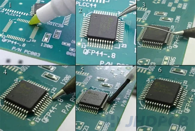
  1. Pad Flux: This pre-solder will help hold the chip in place and ensure that the pad gets enough flux.
  2. Aligning the chip: Add a tiny drop of solder to the clean tip’s end: The secret lies in securing the corners and soldering the rest of the pins. You want a tiny drop of solder hanging off the end of the tip. Too much and you will create a bridge or short between the pins.
    Secure the two opposite corners together: Slide the corner pin’s tip slowly up to its toe. All you have to do here is make contact between the solder drops and the pins. Surface tension will take control once they come into contact and wick the solder off the pins. This is the magic of surface mount soldering. Be cautious to double-check the alignment and, if necessary, reheat the initial pin before pinning another corner. It is nearly impossible to make modifications without entirely removing the chip once many pins have been soldered.Even with a solder core, surface tension will retain a certain amount of solder under the pins.
  3. Add more flux to the top of the pins: You may wish to perform this operation and skip the initial pad flux before fixing the corners.
  4. Continue soldering the rest of the pins: Continue soldering pin by pin using the same technique. With some practice, you can solder an entire row of pins at a time by dragging larger solder dots over the toe – this is called drag soldering. Some techniques designed specifically for this technique are called “hoofing” and “mini-wave” techniques.

A finished QFP chip

The solder paste is applied to the PCB metal pads by stencil printing. To determine the amount of solder paste to be used, you should check the stencil thickness and stencil aperture. Please note that too much solder paste can cause solder bridging. On the other hand, a small amount of solder paste will reduce solder spreading. Therefore, the measurement should be very accurate.

Solder Paste:
Solder paste (lead-free) consists of some type of SnAgCu alloy. The particle size of this alloy must be suitable for the solder stencil aperture size printing.
It is best to use type 4 pastes in this process as they are more efficient. Please also note that solder paste is sensitive to humidity, temperature and aging.
Placement:
The reliable creation of solder joints is supported by self-alignment caused by the liquid solder’s surface tension. However, you still need to place the components carefully. Setting the package manually is not recommended. Instead, we recommend that you use a pick and place machine to ensure accuracy every time.
Reflow Soldering:
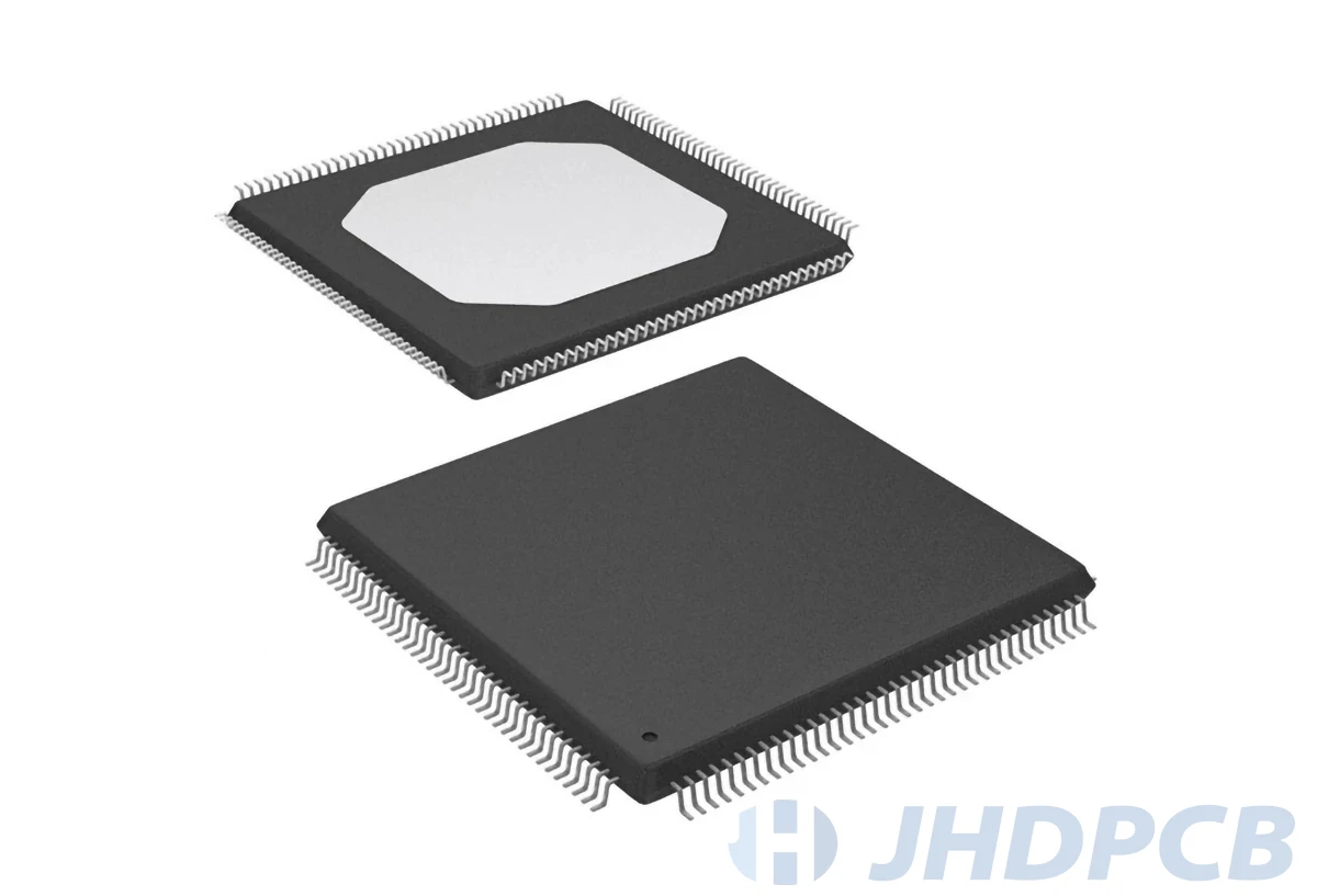
In printed circuit board QFP assembly, you can use a forced convection oven for reflow soldering. Soldering QFPs in an atmosphere filled with nitrogen improves the quality of the solder joints. Nevertheless , this is unnecessary to create reliable joints.

QFP solder joint temperature can be affected by several factors:

  • Its position on the PCB;
  • Is the perimeter;
  • PCB thickness;

For power packages where insufficient QFP down and leakage current are influencing factors, you should use less flux spread for soldering. Remember to follow the manufacturer’s guidelines when soldering for optimal output.

Repair process.

Operators with a light touch and stable skills should be selected for training. Before repairing, determine if the part is salvageable. Not all are salvageable. The pin may be bent so much that it will break if simply bent backwards. These operations should be performed on an anti-static workbench and require proper lighting and magnification. An illuminated magnifying glass with three to four diopters is sufficient.
The operator should select a suitable template and attach it to the plate. There might be some offset, but there should be enough room on the template and plate to handle QFP. The component is placed on the adjustment template.
The technician then selects various tools to make adjustments from coarse to increasingly fine adjustments. Toe and heel adjustments, leveling the foot bar, adjusting the coplanarity, and pulling out twisted and bent pins with tweezers may be necessary for normal operation.
The template is a good tool for aligning pins to the proper spacing. The knees can be put in position without moving the other pins once the pins are in their proper holes. The template is also the best tool for final checking of spacing. The flat plate, with only 0.00002″ of non-planar error, is very useful for toe alignment and coplanarity checks.
During operation, the technician should minimize further bending of the lead. The excellent quality and inertia of metal packing seem to have a tendency to harm the QFP in some way, particularly if the matrix tray experiences any kind of impact. Further bending to keep the ring in a highly fatigued condition should be avoided.

What is the difference between QFP and QFN?

QFN vs QFP package
DifferencesQFNQFP
Lead DifferencesLeads extend to all four sides of the QFN package;Leads extend in a gull-wing or L-shape;
Assembly Section DifferencesAverage foothold of QFN package occurs during PCB assembly;Even during PCB assembly, the lead form provides a good base for the QFP package;
Pin DifferencesQFN packages have a total of only eight pins, plus a thermal pad;QFP packages have multiple pins, ranging from 8 pins per side to 70 pins per side;
DimensionsThe smaller profile of QFN parts allows for smaller overall board size for your project, which is necessary to meet design requirements and provides advantages in PCB manufacturing.QFP package dimensions are typically bigger than their QFN equivalents;
ReworkQFN packages absolutely require the use of a reflow oven;A QFP package’s exposed leads are simpler to handle than a QFN part’s hidden contacts. With a little care, it is entirely possible to hand solder or desolder QFP packages;

If you don’t know which QFP type is suitable for your current PCB application. You can contact our engineers to send your Gerber files, and we will provide the best selection suggestions based on your application conditions, PCB design and production process requirements while conducting a free PCB file inspection. In order to provide customers with a variety of options, JHDPCB company offers qfp packages with pin center distance of 1.0mm, 0.8mm, 0.65mm, 0.5mm, 0.4mm, 0.3mm, etc. The minimum pin center distance is 0.4mm and the maximum number of pins is 348. In order to prevent pin distortion, several improved QFP variants such as bqfp, tqfp, gqfp, etc. are available to meet customer needs. We also use automotive-grade packaging materials and process control to meet sample delivery requirements.

If you want to learn more about printed circuit boards, don’t forget to visit our blog and other PCB production, type related knowledge for more interesting content about the PCB industry. JHDPCB is definitely an experienced and responsible PCB manufacturer.

Get a PCB Quote Now

Open high-quality PCB manufacturing services in JHDPCB

Leave a Comment