How Much Do You Know About PCB Solder Mask?

jhdpcb@gmail.com
What’s Solder Mask in PCB manufacturing?
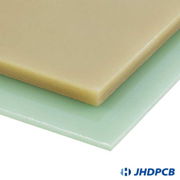
Solder Mask, Solder Resist is a thin protective layer with polymer coating which is applicable to the copper circuits of a bare printed circuit board (PCB) for protecting against oxidation, and to prevent the formation of solder bridges between closely spaced pads.
Next, I will take you to a comprehensive understanding of the relevant knowledge of the solder mask layer. The content includes the following-
Solder Mask Manufacturing Process.
For professional PCB manufacturers, there is no room for sloppiness in solder mask fabrication. for one thing, it accord with strict constitutions such as ISO9001, UL or RoHS must be followed. for another, solder mask manufacturing is divided into some steps, and each process demand,abundant manufacturing experience,the progressive equipment and advanced mature technology. It just so happens that JHDPCB has all these conditions, 12+ years of PCB manufacturing experience and top-notch equipment ensure some smooth progress. Click to view the JHDPCB manufacturing factory.
The general procedure for solder mask fabrication proceeds as described below: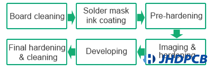
Step 1: Clean The Circuit Board.
The purpose of this step is to wash the surface of PCB board to prevent colour fading or dirt while keeping the surface dry.
Step 2: Solder Mask Ink Coating.
Then put the clean circuit board into the vertical coating machine for solder resist ink coating. The thickness of the coating is dictated by the reliableness prerequisite of the PCB, the region served by the PCB, the thickness of the pcb board and other factors. what’s worse, the surface of the pcb board is not as smoothen as prospective. Solder mask inks vary in thickness when placed on dissimilar parts of the board, such as on traces, on a substrate, or on copper foil. Experienced PCB manufacturers typically specify specific coating thicknesses based on device performance and manufacturing experience.
Step 3: Pre-Hardening.
Unlike full hardening, the purpose of prehardening is to make the coating on the PCB board relatively solid so the redundant coating can be easily cleaned from the board during the development step.
Step 4: Imaging and Hardening.
Imaging and Hardening. At this stage, transparencies with some images of the circuit are mounted on the board and then exposed to UV light. This process hardens the solder mask covered by the clear film segments, while the solder mask covered by the circuit diagram segments remains pre-hardened. Therefore, proper alignment must be ensured when hardening is performed to prevent exposure of unspecified copper foils from creating short circuits or further affecting the final performance of the board.
Step 5: Developing.
The PCB is then placed in developer to remove unwanted solder mask to properly expose the specified copper foil.
Step 6: Final Hardening and Cleaning.
Final hardening is done so that the solder mask ink is completely attached on the surface of the PCB board. The solder mask covered circuit board must then be cleaned before further processing (such as surface finish, assembly, etc.).
4 Main Types of PCB Solder Mask.
All solder mask layers composed by a polymer layer that is to the metal circuits on the PCB printed circuit board. There are many kinds of PCB solder mask, and the best choice for your board according to the price and your practical application. Using silkscreen to print liquid epoxy on the substance that readily conducts is the most common choice . It’s like spraying paint over a stencil with an airbrush. Solder mask can be used with almost all colors.
Liquid Epoxy Solder Mask:
With silkscreen to print liquid epoxy on the PCB board is the most common used. This is the cheapest and most popular option for solder mask. During this stage, a woven mesh is chosen to use for supporting the ink-blocking design. Epoxy liquid is a thermosetting polymer that hardens during thermal curing. Solder mask dyestuff is the commixture with liquid epoxy and solid to any color pointed.
Liquid Photoimageable Solder Mask (LPI):
More advanced solder masks use photolithographic processes with dry film or liquid solder resist, similar to those used for photoresist exposure in semiconductor manufacturing. LPI can be screen printed like epoxy or sprayed onto the surface, which is usually a cheaper method of application. A more sophisticated and precise way is to use a photolithographic technology to specify solder mask openings for pads, and mounting holes and via holes.
Liquid photoimageable solder masks are typically applied to printed circuit boards as follows:
A. The plate surface should be completely cleaned and jerked to guarantee that there are no any detritus on it.
B. Both sides of the plate are completely covered with liquid masks.
C. Place the coated board in the oven to fix the dry mask.
D. The film is made from a solder mask Gerber file. When you want to utilize the mask on the board, the film will be limpid.
E. The dried cardboard is placed into the UV photographic developer and the film and the cardboard must keep in a straight line. The black areas of the film will block the UV rays from curing the mask where it is not needed.
F. After exposing the mask to UV light, rinse off the uncured cover.
LPI solder mask is an material with epoxy, so it is long-wearing and almost impossible to take off after hardening. There are many different kinds ways of using LPISM inks, such as electrostatic spraying,screen printing, air spraying,curtain coating and so on.
Electrostatic coating is a productive process that utilizes electriferous particles to spray workpieces more expeditiously.
Typical powder coating process:
Pretreatment – Spray Baking – Cleaning Check Package
When using air spray, LPI can be performed with a single chip or multiples. This is a traditional spray technique where a thin liquid resistance is mixed with decompressed air at the nozzle of the spray gun. The resulting atomized droplets create resistance, which is then transported to the circuit board by air pressure. Contrasting with static electricity spraying, the spray precept of air spray is somewhat different, and the equipment is also cheaper.
Productivity, overspray losses, and coverage are similar for both electrostatic and air spray. This kit can be used to coat PCB circuit boards in a horizontal or vertical direction.
Curtain Coating – High Speed
Low Material Loss LPI Coating Method:
As PCBs are getting more and more complicated, with wider trace spacing and narrower trace widths, curtain coatings are increasingly used in the circuit industry. With covering coating technology, LPI is applied as the PCB falls from a narrow slot through a sheet or curtain of low viscosity ink. Curtain coatings can use liquid materials at very high speeds with low material losses.
Screen printing, the most common method of LPI solder mask application.
Semiautomatic screen printing application LPISM is the most widely apply of solder mask today. The silk-screening process began to develop rapidly around 1921. Now extremely automated, it has been naturalized in various decorative and industrial sectors including the PCB industry. Of all the printing technologies, such screening process is well supplied to the printed circuit production prerequisites. Relying upon the application, it can deposit resistors on non-etched and etched PCB boards in extensive thicknesses.
Screen print through the tensioned mesh and apply LPI to the board with a squeegee. Ink deposition is controlled by changing the lot of grids and print settings,pressure and speed,A stencil-like image is sustained on a material grid on a rectangular frame. During printing, the structure fills the screen with ink. Then swipe across it with a rubber brush, and the ink flows through the open cells of the grid. At the same time, the substrate is in contact with the screen, and the ink is transferred from the usable portion of the screen to the substrate. Click to view the principle and precautions of PCB screen printing technology.
Dry Film Solder Mask (DFSM):
DFSM solder mask application process is similar to LPSM. Both PCB solder masks are exposed in a photolithography process. Instead of being used as a liquid, the dry film is applied to the solder mask piece by piece using a vacuum substrate process. This vacuum substrate step forces the unexposed solder mask to attach to the board and removes air bubbles from the film. After exposure, the areas unexposed of the solder mask are taken off with a solvent and the remaining film is cured in a heat treatment.
Top And Bottom Masks:
If you consider other guide rules on PCB solder mask types, the two solder mask types that are often referred are top and bottom solder masks. These just refer to definite solder masks put on the top or bottom of the PCB board; they do not allude to a definite manufacturing process or a certain type of solder mask material.
Final Steps: Curing and Surface Preparation.
Using the above media requires cleaning the circuit board to remove dust. After that, they will also go through the final solidify and covering process. Liquid epoxy solder masks are thermally cured without UV exposure.LPSM and DFSM films are solidified by ultraviolet irradiation during lithography. After exposure, these films are solidified and hardened with heating processing.
Regardless of what kind of PCB solder mask you apply, the final solder mask will keep copper exposed on the PCB board. These exposed regions must be surface treated to prevent oxidation. The typical finish is OSP or Hot Air Solder Leveling/HASL(LF), although other popular finishes are Electroless Nickel Immersion Palladium Gold (ENEPIG) and Electroless Nickel Immersion Gold (ENIG) etc. Gain comprehensive knowledge of PCB surface preparation. If applicable, leave additional holes in the mask layer for sticking the mask. The paste mask is used to connect the pad or other components to the PCB board and perform different operations according to the manufacturing process
Solder Mask Thickness.
In order to ensure the quality of the PCB board, it is necessary to select a suitable solder mask and control the screen printing process. In respect of electrical performance, the thickness of the solder mask will greatly affect the safety, impedance, and feasibility of PCB assembly, Therefore, manufacturer must control the thickness of the solder mask strictly.
How To Measure The Thickness Of Solder Mask?
The thickness of the PCB solder mask depends on the material and the type of PCB. In addition, the thickness of the PCB solder mask varies from place to place. The thickness of standard PCB solder mask is 8-15um, and the usual thickness is 10um.
The sprayed solder mask thickness will be slightly thinner, while the curtain covered solder mask thickness will be slightly thicker.
What Is The Effect Of Solder Mask Thickness?
The copper would be exposed that resulting in SMT problems if the solder mask is too thin. According to IPC standards, corner lines are typically larger than 8 microns. Otherwise, it will turn yellow when baked, causing copper to leak.
For the finished copper thickness of 35 µ m, the maximum solder mask thickness can reach up 40 µ M. For higher final copper thickness, the solder mask thickness can be as high as 80 µ M.
If the PCB solder mask layer is too thick, the parts may tilt, affecting the assembly quality and causing IC components welding problems. Thick copper always has thick resistance to welding.
Once we scrape the solder mask on the copper surface with a scraper, it is less prone to scratches. In addition, a good solder mask is not easy to wear due to its good adhesion. Only if someone on the production line is intentionally scraping the solder resist with a sharp metal blade; otherwise, the copper won’t be severely exposed, even with a slightly thinner thickness. The most important thing is whether the adhesion of the solder mask is sufficient.
So most clients will limit the ink usage. Based on the visual inspection criteria, the lower limit is not strictly restrained provided the copper is not exposed ,including disguised exposed copper.
PCB Solder Mask Color and Finish.
Initially, the solder mask was only green. Various colors are now available to make your PCB look attractive. When PCBs have different solder mask colors, it is also easy to distinguish them. The colors are glossy and matte.
JHDPCB Available Colors Include:
Glossy finish-Green, Black, Eed, Yellow, White, Purple, Blue;
Matte finish-Green, Black;
Why Was The Early PCB Solder Mask Green?
For years, the only solder mask color you could see on a PCB was just one color: green. Why is green solder mask is the only early color of solder mask? Why don’t we start with a blue, yellow or red welding mask? There are several possible reasons to consider.
Why PCBs are Green?
- It goes back to an old military exigency that solder masks must be green.
- The solder mask is green because when originally produced, the base resin is tan and the hardener is a very cloudy brown, and when you mix them, you get green. Besides, PCB plates during those period were mostly green. So it’s easy to get the idea of a green solder mask.
- When tested under various adverse conditions, this particular green color contrasts correctly with the white legend ink.
- Green color is the most visible color to the human eye.
White Solder Mask.
A white solder mask cannot address such a small feature as a standard green, or even blue or red solder mask. The reason of the very high pigment loadings is to make white color solder masks. A big number of uncommon white pigments are used in the formula to obtain a bright white solder mask that resists yellowing.
White solder masks are commonly used in LED PCB applications with metal cores. Developers face many challenges when designing printed circuit boards for LED components. On the one hand, the colors presented by the LEDs must be clean and clear. On the other hand, they have to ensure good heat dissipation of the LED components. The white solder mask provides higher brightness for the LED system.
NOTE: If the solder mask is white, white silkscreen cannot be used. Characters can be viewed in black, yellow, red, and other colors.
Why Solder Masks Use Different Colors?
The reflection, absorption or transmission properties of light will affect the assembly equipment. Applications can also create color demands except for green to produce the required contrast or brightness.
Alternate colors can significantly affect the identification of lead-free components, helping to avoid errors in mixed component environments.
The color of solder mask have no influence on the property of PCB itself. But, the difference among different colors is that the resolution power of the board will be different colors such as red and blue, which phase match the resolution of the green PCB. However, the black and yellow solder masks have significantly lower resolution than the green ones, while the clear solder mask has a higher resolution.
Main Types of Solder Mask Inks.
Due to the fast development of the PCB industry, PCB ink makers have gained more opportunities.
The PCB solder mask ink industry is a high-tech industry, involving UV curing technology, ultra-fine powder applied technology, lithography technology and coating and ink production technology. Some products must have high temperature resistance solderability above 280℃, line accuracy performance of 25 microns, electroless nickel plating, tin resistance, electrical insulation performance above 1011 ohms, high voltage breakdown performance above 20kV, UV sensing optical performance .
PCB ink needs to reduce environmental pollution and harm to operators with feature of environmentally friendl,safe,low-toxic and odorless.
Some solder mask ink manufacturers and specialists have started to develop non-toxic solvents. Many ink buyers from different countries have started to buy solder resists from Chinese PCB ink manufacturers, which shows that Chinese PCB inks also occupy a specific international market. More opportunities mean more challenges. It improves China’s PCB ink manufacturing technology and leads the development of related technologies and other related products.
Some solder resist ink manufacturers and experts have begun to develop non-toxic solvents. Many ink customers from all over the world have begun to purchase solder resist from Chinese manufacturers, which indicates that Chinese PCB ink also hold a specific international market. More opportunities that’s also mean more challenges. Improving manufacturing technology of China’s PCB ink and leading the development of relative technologies and other correlative products.
Commonly used solder mask inks are: *Thermal curing solder mask ink, *UV Curable Solder Mask Ink, *LPI Solder Mask Ink.
Characteristics of PCB Solder Mask Ink:
Describe 10 features of PCB solder mask ink-
*Viscosity, *Plasticity, *Thixotropy, *Fluidity, *Viscoelasticity, *Dry, *Accuracy, *Harsh, *Transparency And Opacity, *Safety And Environmental Protection.
What Is Peelable Solder Mask?
Peelable Solder Mask (PSM): Peelable Solder Mask PCB is a printed circuit board with a peelable solder mask (temporary solder mask) to protect certain areas during surface preparation or assembly. This is to say, sometimes PCB boards require protection of selected areas of the board during surface preparation or assembly to prevent solder flow onto plated through holes, terminals, and other connection.
Strippable Masks: also known as strippable masks or blue masks, are used on soldered mask PCBs to protect circuits by screen printing. A peelable solder mask make protecting in welding processes such as reflow soldering,wave soldering, and HASL(LF) surface.
When these processes are complete and the solder mask is no longer needed, it can be removed mechanically or “stripped” manually. This area is used to protect exposed parts during final assembly. Peelable masks are not a substitute for standard solder resistance.
Advantages of peelable solder mask:
*Reliable, time-saving and money-saving
*Protect shapes by screen printing
*Protect selected areas on the PCB
*Easy to remove, no residue
*High temperature resistance
Solder Mask Bridge Broken Pads.
The solder mask between the different soldering pads is called a solder mask bridge , which prevents bridging or direct short happened during soldering. In many PCB factory, solder mask bridge breaks lead to product poor quality and production non-efficiency. The requirements from customers are getting higher and higher by the fast development of the PCB industry. Time to increase the processing power of the solder mask bridge.
What are the factors that affect the disconnection of the solder mask bridge?
Ink Light Transmittance:
The main reason for the disconnection of the solder mask bridge is that the UV intensity decreases rapidly with the light transmission depth of the solder mask ink. When the ink exceeds a certain thickness, it does not fully photopolymerize, so undercut and solder mask bridge breakage can occur during development. At the same time, exposure energy, development time, pre-curing time, etc. will affect the disconnection of the mask bridge.
Exposure To Energy:
At the same exposure, as the thickness of the solder mask increases, the amount of undercut of the solder mask bridge increases. There was also a break in the solder mask bridge, and the production capacity of the solder mask bridge decreased. When exposed to UV light, part of the UV light is absorbed by the liquid photosensitive solder mask ink.As a result of absorption, the strength of ultraviolet rays gradually decreases, so its energy is getting weak while the UV light range to the bottom side of the ink. Therefore, when the ink accumulated to a certain thickness, the bottom of the resin will not be in a state of incomplete photopolymerization,it caused undercuts during development.
When the primer is not fully photopolymerized, increasing the exposure energy can lead to better photopolymerization of the primer, thereby reducing undercut. But it’s difficult to carry it off. In the real manufacturing of PCB circuit boards, the exposure energy cannot be increased infinitely.
Developing Time:
When the solder mask is thin, such as 25-50um, it has little influence at the undercut of the solder mask bridge; when the solder mask is thicker, such as 70-75um,it has big influence on the undercut of the solder mask bridge. With the shortening of the development time, the undercut resistance of the solder is significantly reduced.
Pre-Curing Time:
When the solder mask is thin, such as 25-50um, the pre-curing time has little influence on the undercut of the solder mask bridge; when the solder mask is thick, such as 80-85um, the pre-curing time has big influence on the solder mask bridge. By the pre-cure time increases, the solder mask width increases and the undercut decreases.
Other Factors:
Such as pre-cure temperature, development pressure, developer potency, and development temperature, can also affect undercut and solder mask bridge breakage.
In Conclusion: When the ink build-up a certain thickness, it does not fully photopolymerize because the intensity of the UV decreases fastly with the depth of transmission of the solder mask ink, so undercut happened. Solder mask bridge breaking available during development.
Increasing the exposure energy can lessen undercut.
Development time, pre-cure time, pre-cure temperature, development pressure, developer concentration and development temperature also affect undercut and solder mask breakage
What Is The Difference Between Solder Mask And Paste Mask?
Many people may be bewildered between solder mask layers and stick mask layers because they have some similar features. This article will explained the difference between solder mask and solder paste mask and make you better understand.
Here are some of the differences between solder masks and solder paste masks:
- The opening on the solder mask layer has no solder mask ink, but the opening on the paste mask layer has paste.
- Solder mask is part of the board, but paste mask is not. Paste mask layers are only used for stencils.
- A solder mask is used to apply solder mask ink, but paste mask is used to apply paste.
- Use solder mask when making PCB board, but use paste mask when assembling.
- Solder mask comes in a variety of colors, but paste mask is usually gray.
How To Repair The Solder Mask?
Generally speaking, after curing, the solder mask is not easy to peel off. The solder itself is resistant as a protective layer for the printed circuit board.Now list some ways to repair solder mask damage on the PCB.
You can use a particular solder mask repair pen to apply ink on the PCB board. Then make it dry in the oven.It can be baked at 150 ℃ for 20-30 minutes if the PCB board without assembly. You can bake it at 120 degrees for about half an hour if it’s already assembled. It dries in short time in the oven. Maintenance pens are usually simple to use and ink masks are durable.
If it’s just for aesthetics, you can fix the board with something like oil-based crayons. But this only improves the appearance temporarily, without the thermal insulation and protection effect.
- Summing up the BGA solder mask repair steps as the following points:
*Clean the area to ensure adequate adhesion, optimize electrical performance, and minimize corrosion effects.
*Remove all extra solder on BGA pads.
*Scrape or grind.
* Prepare replacement solder mask material.
*Use coating instead of mask material.
*Let the epoxy cure in the oven.
*Confirm that repairs have been done correctly by checking the electrical continuity of the vias and the BGA pads.
How To Do Testing For PCB Solder Mask?
We know that solder mask is commonly used on PCB boards. After the solder mask process, it is sometimes necessary to check for any solder mask issues. (For a complete pcb board test, please move)
Direct visual inspection, then use 1.5 to 10 times magnifying glass.
Test peel strength with 3M tape according to IPC-TM-650/TM2.4.28.1 standard.
According to IPC-SM-840C 3.5.1/TM 2.4.27.2 standard, draw a one inch long line on the board with pencil hardness (JIS standard) after baking and use about one inch at an angle of 45°C.
According to IPC-SM-840C 3.6.1.1 standard, take two 6PNL silver test plates, and immerse each test plate in 10% hydrochloric acid, 10% sulfuric acid, 10% sodium hydroxide solution for 30 minutes. Two other 6PNL OSP plates were then immersed in a solution of 10% hydrochloric acid, 10% sulfuric acid, and 10% sodium hydroxide for 60 min. Then checking the surface for peeling, blistering, discoloration, etc.
According to IPC-SM-840C 3.6.1.1 standard, clean the surface of the coating and check the surface for blistering, peeling, discoloration, etc.
1) Soldering: According to IPC-SM-840C.
2) Soldering resistance: in line with IPC-SM-840C.
3) Solder heat resistance.
4) Tin bleaching test: temperature: 260℃, time 10S, test three times.
Take several sections of silver and OSP board and measure the thickness of ink at different positions.
Measure whether the undercut depth is within 1.2 mm.
According to IPC-SM-840C 3.9.3/TM2.6.7.1 standard, H degree, 65~125°C, 100 cycles, check the surface for blistering, peeling, discoloration.
Design 2mm, 3mm, 4mm, 5mm solder mask on the negative film (according to different process capabilities). After developing, baking, FQC, check if it is turned off.
How to distinguish solder mask, Surface Finishes and conformal coating?
For a novice, it is easy to confuse solder mask with surface treatment and conformal coating. But in fact they are very easy to distinguish.
- Solder mask is used to protect bare board circuitry and pads. Prevent the possibility of oxidation and subsequent solder bridges on the exposed circuit of the board.
- Surface Finishes are the coating between the component and the bare PCB. Used to ensure the solderability of ic assembly, improve the reliability and shelf life of PCBA.
- Conformal coating (Conformal paint) is a comprehensive protection process implemented in the final stage of circuit boards. Protect PCB functionality and its components from potentially damaging environmental conditions. It acts as an insulating layer while protecting the surface of the PCB.
Through the above JHD explanation of the knowledge of pcb solder mask. I believe you already have a deep understanding of PCB solder mask. If you want to know more about other processes in the PCB manufacturing process, please check our other articles or contact us. With years of experience and strong production strength, JHD can definitely give a satisfactory answer to your PCB needs.