Impedance Control on PCBs: What for/ How to control/ Impedance calculation

jhdpcb@gmail.com
- Release Time: 2022-07-26
directory
What is pcb impedance?
Common sense impedance control is a force and position dependent physical dynamic control method. It defines the motion that force produces. The impedance control in the printed circuit board expresses the control of the circuit board trace width and height, dielectric materials and other production process factors on the circuit signal propagation.
Impedance measures the impedance of a circuit when alternating current is applied. It is a combination of capacitance and induction in a PCB circuit. Impedance affects how signals travel through the board, how power is transferred between components, and how signals flow into unwanted areas of the PCB. Impedance may vary with operating frequency. The impedance formula is usually represented by Z = R – j/ωC + jωL, where ω = 2πf. Transmission is optimal when a signal is passed from a conductor with a given impedance to another conductor with the same impedance. On the other hand, if the impedances are different, reflections and attenuations that degrade the signal will occur.
The difference between impedance and resistance.
Impedance is measured in ohms, similar to resistance. However, these two values should not be put together because resistance is a characteristic of direct current. That is, the resistance can limit the DC circuit and the AC current, and the impedance can only limit the AC current. Impedance has no meaning in a DC circuit.
| Resistance | Impedance |
|---|---|
| R | Z |
| Two or more resistances in series can be added arithmetically. | Vector addition should be performed to sum up the impedances. |
| Unaffected by the supply frequency. | Mainly depends on supply frequency. |
| Current through resistance is always in phase with the voltage across it. | Current and voltage are out of phase. The phase difference depends on the inductance or capacitance present in the impedance. |
What is an impedance control?
Impedance control, there will be various forms of signals that need to be transmitted in the PCB, and the overall transmission rate can be increased by increasing its frequency. The circuit itself will have different effects on the impedance value due to different factors such as the physical size of the PCB, dielectric materials, etching, stack thickness, and line width, and the signal will be distorted. Therefore, the impedance value of the conductors on the high-speed circuit board should be controlled within the limited range of the PCB design, and ensuring the signal stability of the PCB is called “impedance control”.
Importance of Impedance Control.
Good impedance control allows the PCB to perform faster and more stable operation with less energy. Thereby increasing product value and stability. In some specific areas, PCB circuit signals require specific impedances to function properly. Examples include RF communications, telecommunications, high-quality analog video (eg DDR, HDMI, Gigabit Ethernet) and , electronic devices that use high frequency signals above 100MHz.
In the process of high-frequency signal transmission, the circuit traces on the PCB play a role in transmission, and each point on the trace has a specific impedance value. If the impedance changes from one point to the next, signal reflections will occur. Reflections will travel in the opposite direction of signal transmission, which will alter the integrity of the original signal. Its magnitude will depend on the difference between the two impedances, too much difference will cause the signal to possibly not perform the desired function.
Therefore, impedance matching keeps the impedance constant across the board for protecting transmitted data from damage and maintaining signal clarity. PCB signal traces must have uniform controlled impedance, and longer traces or higher frequencies require more adaptation. to minimize signal distortion caused by reflections. Proper PCB design layout is the first step in improving signal integrity on PCB traces.
How to do impedance control in pcb?
There are currently five methods that enable efficient impedance control in a PCB:
- Give clear signals during PCB design.
It is a good rule of thumb for the PCB designer to specify which signals require impedance control at design delivery.
A component data sheet is also included and provides information on each component’s signal class and corresponding impedance values.
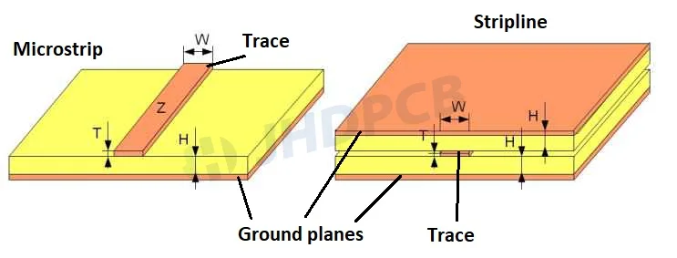
Also indicate which layer is more appropriate to pass individual signals and which spacing rules must be used between traces. - Choose the appropriate transmission line form: microstrip line and stripline.
Microstrip line is a circuit line widely used for high frequency transmission, such as antennas, filters and power dividers. A microstrip line for the outermost layer of a PCB is an electrical transmission line that can be fabricated using printed circuit board technology to transmit microwave frequency signals. Microstrip devices can be built on common FR-4 substrates in order to reduce cost in common applications. It consists of conductive strips separated from the ground plane by a dielectric layer called the substrate. The resistance capability depends on the dielectric constant, the thickness of the insulating material, the width and thickness of the traces. These factors affect the impedance value, so the operating frequency of the circuit should also be selected in the design stage.
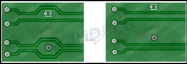
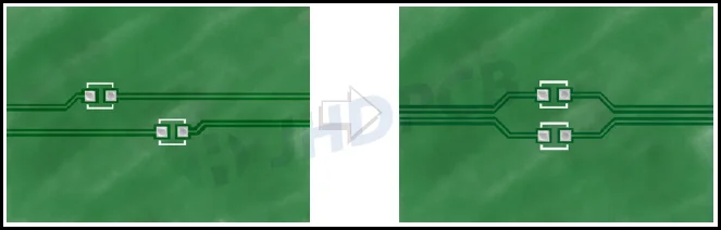
- Ensure that all the traces and components on the PCB have a certain distance.
During PCB design, impedance-controlled traces should be properly spaced from other traces and various components on the PCB to eliminate crosstalk as much as possible. This phenomenon generally affects microstrip lines. Therefore, we recommend that the minimum spacing should be “2W” (W represents the line width of impedance control), and “3W” is the best if conditions allow.
When it needs to be applied to the scene of transmitting high frequency signals, the minimum distance should be increased to “5W”. Keep at least 30 mils away from any other type of trace for better isolation. - Unify the length of the traces.
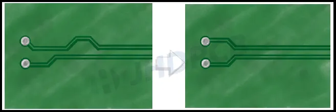
Unifying the length of the traces during signal transmission avoids the delay of the signal frequency (this is based on the fact that all traces are kept constant). It is especially important in a high-speed propagation signal group to ensure that all signals can reach the destination at the same time.
If the signal comes from a different point, a serpentine is usually inserted in the shorter trace to compensate for the length relative to the other traces. - Control the use of capacitive components.
If you can try not to use components and capacitors between signal traces, any component will have some filtering interference in the impedance value. If placement of capacitors is unavoidable, they should be placed symmetrically to achieve signal unity across all traces.
how to measure pcb trace impedance?
I believe that you should have learned that impedance will affect the propagation of signals in the PCB through the above introduction. It is not visible by itself, so some method must be used to make circuit impedance measurements.
- Analog circuit.
Verify board design functionality in a PCB design software program after the PCB design is complete. Many design programs can simulate real use based on the proposed values of all physical dimensions, materials, line widths, components, dielectric materials, stack thicknesses, etc. of the PCB. Then measure the PCB circuit impedance. - Online calculator.
At present, there are many online impedance calculators on the Internet. Although it is not as detailed as analog circuits, it can calculate impedance control values and routing parameters based on empirical formulas. Of course, most calculation tools cannot take into account the trace shape and dielectric material. This method can only give an approximate value to help you make certain numerical adjustments before manufacturing. - Instrument measurement.
After the PCB manufacturing is completed, the actual circuit passing test is carried out using an impedance measuring instrument. The real signal transmission stability of the circuit board can be measured. Of course, instrument measurements do not cover later assembly components and usage environments. The lead length, current passing, and ambient temperature of the component will all have different degrees of influence on the impedance of the PCB under real use conditions. The common method is flying probe test. For specific information, please refer to the JHD PCB test content.
How to calculate impedance in a circuit?
When we want to obtain circuit impedance by manual calculation, we need to use some inherent calculation formulas.
When there is no component installed on the circuit, the circuit impedance calculation formula: Z=√(L/C).
L is the inherent inductance of the circuit per unit length, and C is the inherent capacitance of the circuit per unit length. To change the characteristic impedance of the transmission line, it is necessary to start with the inherent inductance and capacitance of the circuit per unit length.
There are many factors that need to be considered when calculating the impedance of a PCB circuit. You can use the following PCB impedance trace formula to calculate its circuit impedance:
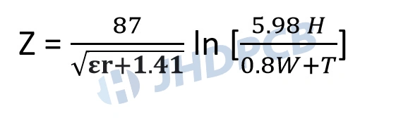
εr : The dielectric constant of the material;
H: The height of the insulating material between the trace and the surface of the substrate;
W : The width of the trace;
T : The thickness of the trace;
Whereas, when linear components are included on the PCB, you need to know the capacitance and circuit impedance of all components that affect the circuit impedance.
Basic electronics principles such as Ohm’s Law and Kirchhoff’s Law can be used for analysis to determine the impedance, voltage, and current of a circuit.
For a series circuit, the total impedance can be calculated by the following formula:
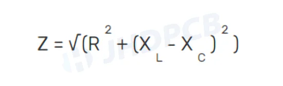
Since both capacitive and inductive reactance are functions of angular frequency, the total impedance is expressed as a complex number with real and imaginary parts.
This is a common expression for circuit impedance: Z = R + jX.
Impedance calculations become more difficult when the circuit contains amplifiers, transistors, diodes, and other components whose output is a nonlinear function of the strength of the input signal. When the input signal strength changes, the transimpedance of each nonlinear circuit element and the equivalent impedance of the circuit also change.
For more complex circuits and circuits with nonlinear components, more advanced simulation and analysis techniques are required to determine the impedance of analog signals in the circuit.
What are the factors that affect impedance control?
I believe that some friends have been able to guess what factors affect the circuit impedance from the above PCB trace impedance calculation formula. The following will list all the factors that affect the impedance of PCB traces:
- The width (w) and thickness (T) of the trace;
- The dielectric constant (ER) of the board prepreg;
- Thickness of insulating material between traces (H);
- Manufacturing process tolerances; (plating tolerances, etching tolerances, presence or absence of solder resist, via resistance, etc.)
- Impedance of the component;
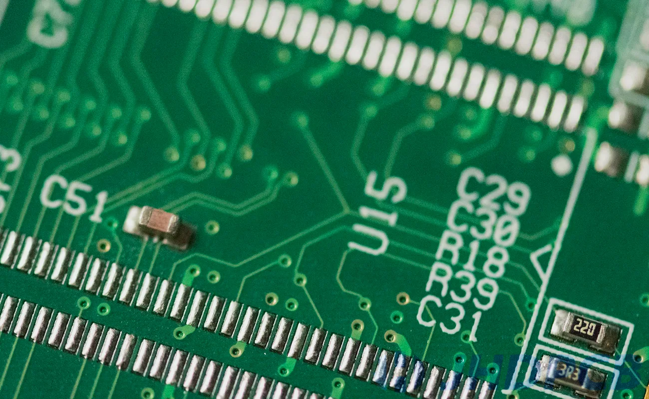
Trace width and thickness:
On a PCB, the trace copper foil width and thickness are critical. As the trace width and thickness increase, the impedance gradually decreases. The following figure shows the relationship between impedance and traces (width and thickness):
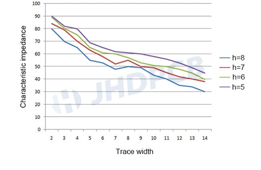
As can be concluded from the figure, the impedance changes dramatically with the trace width. But when designers are designing a PCB, they define the traces based on several different factors, including temperature control and current capacity. Everything is designed based on the expected impedance specific to the board. Therefore, in the production process, it is necessary to ensure that the trace width meets the conditions. In normal PCB manufacturing, if copper foil with a width tolerance of 18μm is selected as the signal transmission to control the impedance, the allowable trace width tolerance is usually ±0.015mm. If copper foil with a width tolerance of 35μm is selected, the allowable trace width tolerance is ±0.003mm. JHDPCB pays special attention to the control of manufacturing tolerances to ensure that the normal use of the PCB design is met.
Dielectric constant of board prepreg:
Choosing the right material to fit is also key to controlling the impedance, the dielectric constant (Dk) of the prepreg material directly affects the impedance value. Materials with stable, low dielectric constants are easier to control impedance. The thickness and resin content of the material are two key factors that determine the dielectric constant of the material, and the Dk value decreases with increasing thickness. Therefore, we give the following suggestions to help you choose the right material for impedance control:
Try to choose a substrate with a high resin content – the higher the resin content, the lower the Dk value. Reduce impedance variation.
Try to choose a material with a low dielectric constant – the lower the Dk value, the better the signal transmission speed and stability. Especially suitable for high frequency applications.
Try not to use more than three types of prepreg materials in the layer stack. The increase in stacking of different types of substrates also comes with increased risk. This is not conducive to the calculation of the dielectric constant of the overall thickness. Read the CCL article to learn more about PCB substrate classification, quality standards and JHD prepreg manufacturing capabilities.
Thickness of insulation material between traces:
This is easy to understand. The increase in the thickness of the insulating material between the circuit traces will also increase the impedance capability to a certain extent. Note that it is generally not recommended to reduce the thickness of the insulating material if it is necessary to reduce the impedance. The reduced thickness of insulating material means an increased risk of signal crosstalk, especially in high frequency signal applications. Therefore, under normal circumstances, other methods are preferred for impedance control.
Manufacturing Tolerance:
The thickness of the coating also has an effect on the thickness of the trace, so the surface treatment is especially important. Remove surface contaminants before electroplating to avoid unevenness that affects impedance consistency.
The chemical corrosion of the circuit by the etching process directly affects the width and thickness of the traces. Control over etching tolerances is equivalent to control over traces.
In some special board manufacturing process, if the etching is carried out after electroplating. That electroplating copper will directly affect the copper thickness of the circuit, and the impedance value will also change accordingly. At this time, it is necessary to pay special attention to the tolerance control of electroplating.
Vias and vias in multilayer board and HDI PCB manufacturing interact with each other between connecting conductive elements. The impedance of the vias is generally between 25 and 35 ohms. Therefore, there is an interaction between the via and the circuit impedance. When vias are placed on circuit traces, noise coupling occurs that affects impedance stability. Therefore, it is necessary to avoid placing vias between differential pairs during design. For more hole types read “Do You Know What Types Of Holes On PCBs?“
Assembling the electronic components:
The impedance of the circuit is also affected by the placement of the components. Resistors, capacitors, and inductors are some of the basic circuit elements.
The resistor is affected by the current, and the resistance value is independent of the frequency of the power supply. Its impedance is the measurement of its resistance:
Z = R
Normally, the reactance of a capacitor is inversely proportional to the angular frequency of the signal. The capacitive reactance decreases with increasing frequency. The impedance of a capacitor is equal to its capacitive reactance, and the impedance of the capacitor is calculated by the formula for the frequency of the input signal:
X c = 1/2 πfC
Inductors work similarly to capacitors, but they provide a circuit impedance that is proportional to the signal’s angular frequency. The formula is as follows:
X L = 2πfL
These are the basic components most commonly related to impedance calculations, but they are not the only components in a PCB. In a design, there are also transistors, ICs, diodes, and other passive components that all bring varying degrees of impedance to the circuit.
PCB Impedance Design Guidelines.
How to formulate an impedance controlled PCB?
Applying a complete impedance control strategy in the early stage of PCB design will help PCB design and production go smoothly.
First, it is necessary to determine which signals on the PCB require specific impedance control. And a detailed data sheet is developed to provide impedance value information for each group of signals. Both signal ratings and trace spacing rules can be included in data sheets or production documentation.
The designer must then specify the impedance control signal in the schematic. Determine the signal type as a single-ended network or differential pair, and add N and P polarity indications for the differential pair circuit. When designing according to the required signal impedance value, you need to specify the values of several important parameters:
- The number of board layers;
- PCB trace width;
- PCB trace height;
- The specific impedance value of the layer where the trace is located;
- The dielectric constant of the base material;
- Thickness of insulating material;
- Tolerance requirements for specific production processes;
- The spacing of components on the trace;
Adding detailed parametric diagrams to specify impedance control will provide a clear specification for the PCB manufacturer’s subsequent production process.
If the designer fails to document these parameters to specify impedance control, delays in lead time can occur. For example, manufacturers faced with vague specification documents for multilayer boards are not sure whether to require impedance control on all layers or only in certain layers; or the documentation given does not provide full detailed impedance control specifications. Such as copper weight, layer thickness and trace width without specified tolerances, etc. The lack of any information will affect the overall delivery time, and even cause the signal loss of the circuit board or the inability to use it normally, resulting in inestimable economic losses.
Best advice for impedance control design.
When the designer specifies impedance control, the error rate should be minimized to ensure the timeliness and quality of PCB production. Here are some common impedance control recommendations:
Parameter labeling: As mentioned above, all factors affecting impedance control are sorted and summarized in the early stage of design. Labeling in design layers when necessary helps to control the manufacturing process.
Controlled impedance traces should be distinguished from other traces: Distinguishing impedance-controlled traces helps subsequent PCB manufacturers quickly identify them. If necessary, the trace width and height can be changed faster and more accurately to achieve a specific impedance value.
Keep the trace width consistent: Under normal circumstances, each PCB layer can only have a uniform trace width. If your spec document calls for two different width traces of the same impedance on the same layer of the board, the PCB manufacturer will have to stop production and ask you which value to use. This will seriously affect the delivery time.
Spacing between traces: Determine the minimum spacing that should be followed between PCB traces based on signal transmission standards and the dielectric constant of the material. To control the impedance line and other circuits will not interfere with each other to ensure the integrity of the signal. There should be different minimum spacings for the same layer and for different layers.
Ensure the symmetry of the traces: Especially in the differential pair signal traces, the same spacing and traces between the signals are beneficial to calculate the impedance.
Specify Layers Explicitly: Sometimes your specification document may only have impedance control for a specific layer of the PCB. And if you don’t specify which layers are targeted, the PCB manufacturer may assume that the document applies to all layers. This will result in a lot of unnecessary work and severe delivery delays.
Placement of vias and components: All placement of holes and components should not interfere with the PCB traces. Avoid inconsistent trace distances, trace asymmetry and adding unnecessary traces. Any circuit change will affect the circuit impedance.
At the same time, if a capacitor needs to be placed in series on the circuit, it is necessary to comply with the symmetry rule. This ensures impedance continuity.
Uniform trace lengths: Differences between trace lengths can also affect impedance uniformity when other factors such as circuit width, height, and dielectric constant are consistent. The unification of circuit lengths thus allows control signals to arrive at their destination at the same frequency at the same time. Sometimes there may be a certain difference in the straight-line distance between signal points, we can use serpentine lines in shorter traces to compensate to ensure the unity of impedance.
Reasonable impedance target: The impedance tolerance is normally controlled within the range of +/- 10%. Tighter impedance tolerances are generally more expensive, as small tolerances that are normally allowed can also result in significant rework. Therefore, please control the cost by specifying the most appropriate impedance target based on the project requirements.
Correct trace path: The impedance circuit should not be affected by other manufacturing processes or affect other manufacturing processes when designing the circuit. Such as: avoiding cut lines, using stitching capacitors to link two different reference planes, staggering vias, etc.
Consistent Annotation and Overlay Design: Ensure consistent information across all document submissions. Avoid inconsistencies between the stack-up design in the software and the specification written in the specification note document. All inconsistencies in information will result in delayed delivery.
Each order received by JHDPCB will be scanned and checked by schematic diagram before production to ensure that all impedance designs conform to the PCB target application and the integrity of signal transmission. This is conducive to the smooth progress of the project. If you have any questions about PCB impedance, please feel free to contact us, JHD will try our best to provide the best solution.