PCB etching

PCB Etching Technology and Solution

directory

What is PCB etching?

PCB etching is one of the major steps in the chemical processing of subtractive printed circuit board. It involves the removal of unwanted copper from a printed circuit board, to achieve the desired circuit pattern. The layout for the board need be generated before the PCB copper etching.

How does PCB etch work?

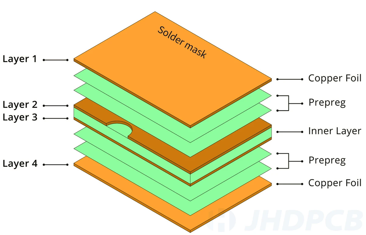
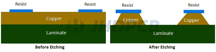
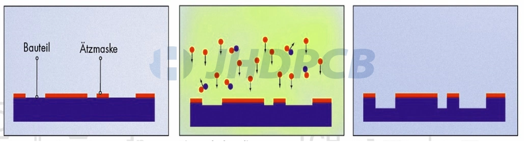
During the PCB etching process, all but the copper plated with tin before etching was removed. Then tin is peeled off and copper is cleaned. This is completed by applying a temporary mask, which protects the circuitry on the laminate from chemicals and keeps the required copper layer unchanged.

how pcb etching works

The Importance of PCB Etching.

Proper PCB board etching techniques have always been of great importance as etching is one of the most important processes in PCB manufacturing. PCB manufacturers use etching to determine the amount of copper remaining on the laminate, which defines the copper pads and traces that make circuits on the laminate. This is related to whether the final PCB circuit can be used or not.

What is the etching process in PCB manufacturing?

The hardened photoresist on the copper inner layer protects the traces, vias and other areas of the metal circuit, and the remaining photoresist is removed to expose the bare copper. Etching is then performed to remove unprotected bare copper, leaving the required circuitry. After removing the hardened photoresist, only the copper circuit remains in the inner layer. Repeat this step for each pair of inner layers until all layers are complete. The next step is to laminate all the inner layers with the epoxy-impregnated fiberglass board, called the “prepreg.” Once the top and bottom of the board are covered by a thin layer of copper foil, the board can be laminated together by heating and pressure. Once laminated, a through-hole is drilled in the plate to prepare for the next etching process. Click to learn more about PCB drilling.

How to etch a PCB board?

Generally, PCB board etching processes can be divided into two types: Wet etching and Dry etching.

Wet Etching:

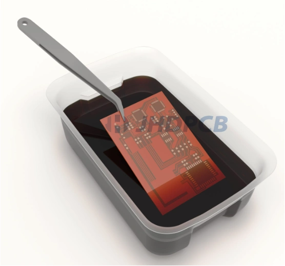
Wet etching is usually done with an acid solution to dissolves the unwanted copper based on chemical reactions. Successful Chemical Etching lies in the selection of an appropriate chemical solution and etch material. There are two kinds of chemicals for us to choose.

Wet Etching

Acidic Chemicals: Ferric Chloride (FeCl3) / Cupric Chloride (CuCl2).
Acid etching is a very efficient process that involves removing copper from any inner layer of the FR-4 circuit board. Acid etching is used for these types of plates because of how precise etching can be. The acid in the PCB etching fluid does not react with the photoresist, which means that the metal does not have as much undercut. The only disadvantage of this type of copper etching pcb is that the acid etching process takes longer to complete than alkaline etching and other methods.

Alkaline Chemicals: chloride copper (CuCl2 Castle, 2H2O) + hydrochloride (HCl) + hydrogen peroxide (H2O2) + water (H2O).
Basic etching can be applied to the outermost layer of a circuit board. Since alkaline etching can be done faster than acid etching, you don’t need to worry about any residual copper uniformity being damaged. Due to the composition of the alkaline solution, it is considered more active than the acidic solution, which means that careful monitoring is required to ensure the accuracy of the etching process.

These two types of etching processes have proven to be effective because large volumes of etching can be performed at lower operating costs. Acid and alkaline etching can also be used with many different metals.

Dry Etching:

Dry etching processes typically use plasma to activate chemical reactions between the substrate and surface atoms of the laminate, which can dissolve unwanted copper. Dry etching is not limited to plasma etching, laser etching PCBs can also be used for the process.

Plasma Etching:
Plasma etching is one of the main applications of plasma treatment. The process is designed to help reduce liquid waste disposal in the manufacturing process and enable selectivity that is difficult to obtain with wet chemistry. During plasma etching, a highly energetic and reactive substance produced by a selected process gas (e.g. O2 or fluorine-containing gas) bombards the sample surface and reacts with the sample surface, with the result that the surface material is broken down into volatile and/or smaller molecules that are then removed by the vacuum system. Part or the entire top layer of the surface can be etched. Therefore, plasma etching is a dry and clean process that does not require any chemicals. Most importantly, plasma etching enables controlled and precise etching on very small scales. It is also particularly popular because it reduces the possibility of via contamination or solvent absorption. Nonetheless, the plasma etching is costly. The chemical properties of the process gas determine how its plasma reacts with the surface of the material, and thus the effectiveness of plasma etching.

Plasma Etching

Laser Etching:
PCB laser etching process allows the use of precise computer-controlled hardware. In this process, a high-power laser engraves a trace on the PCB’s substrate. These unwanted copper traces either evaporate completely or peel off from the PCB. One of the main advantages of laser etching is that it minimizes the number of steps in the process. It also eliminates the need to use any ink, acid or toxic chemical. However, it is difficult to etch evenly on large plates, and it is difficult to handle if the etching agent and residue do not evaporate completely. On top of that, as with plasma etching, the laser etch PCB process is very expensive. The above is PCB laser etching information.

Which chemical is used for PCB etching?

The principle of wet etching is to dissolve unwanted copper by chemical reaction. Depending on the etching material, either acidic or alkaline chemicals can be used in this process.
Chemicals for acid etching usually are: Copper Chloride, Ferric Chloride.
Alkaline etching chemicals are: Copper Oxide, Hydrochloric Acid, Hydrogen Peroxide, Ammonium Sulfate, Sodium Sulfate.
Below, we will illustrate two chemicals.

In the PCB industry, ferric chloride is not used as much as copper chloride because of the high cost of disposing of hazardous waste from the process. But ferric chloride is easy to use and has a strong copper carrying capacity that can be used to handle infrequent batches. Ferric chloride can be used with screen inks, photoresists, and gold patterns, but not with tin or tin-lead resists. Typically, the solution of ferric chloride is dissolved in water at a concentration of 28-42% by weight. HCl (up to 5%) is mixed with this solution to ward off the formation of ferric hydroxide (insoluble precipitate). The commonly used specific gravity of ferric chloride is 36 Be, or about 4.0 lbs/gallon of FeCl2. For commercial purposes, HCl content will be between 1.5% and 2%.

Sodium Persulfate PCB Etching:
An ideal alternative to ferric chloride for a compound used in printed circuit board etching and copper pickling. It dissolves easily and does not crystallize from solution. It is evenly etched, ensuring the sharpness of the contour and minimizing the undercut.
Ammonium Persulfate PCB Etching:
Ammonium persulfate is a copper etching compound, an alternative to ferric chloride, that produces a cleaner copper etcher solution. It allows visual inspection of the etching process, is compatible with tin etching resists, is a non-staining solution and is carbohydrate-compliant.

Copper chloride is the most widely used etching agent because it can accurately etch smaller characteristic copper chloride processes that also provide a constant etching rate and continuous regeneration. Lower relative cost. The maximum etching rate from gold copper is formed by a combination of: Copper chloride – sodium chloride – hydrochloride system. The combination has a maximum etch rate of 55s for low-zinc copper at 130F. Therefore, this type of etching is used to etch the inner layer of fine lines.
Note: When using chlorine, make sure to do so in a well-ventilated room and make sure to use the following equipment:

  1. PCB etching tank;
  2. Cylinder storage;
  3. Leak detection equipment.

What factors determine the quality of etchants?

Ideally, the etching rate depends on the etching time and the etching composition will be constant. However, in practice, the composition of the etching agent is constantly changing. Therefore, in order to guarantee the quality, we must control some parameters. The following are the parameters used to evaluate the quality of the etching agent for smooth operation of the etching process.

  • Baume;
  • Temperature;
  • Redox potential (ORP);
  • Chemical additives (free acids);
  • PH.

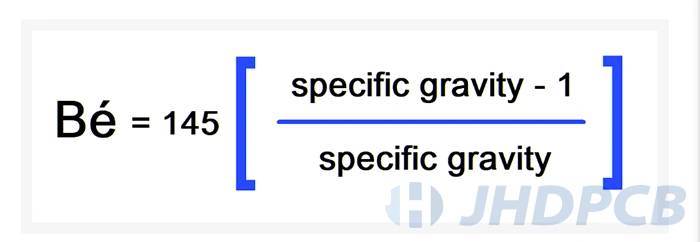
Baume, or Be, is the molar concentration of the etching agent, which depends on the gravity of the solution. High Bes usually coincide with high etchant molar concentrations and ultimately high etching rates. The low Baume degree of the solution means that the molar concentration of the solution is low, which means that the chemical has a low etching rate. It also reduces the number of undercuts formed after the etching process PCB. Therefore, Baume is a key parameter to consider when etching PCB.

Equation for calculating Baume of etchant

Generally, high temperatures will increase the etching rate of the etching agent. But because the parts of the etching machine are not metal (to prevent the metal parts of the etching machine from also reacting with the etching solution) but plastic, the temperature cannot be raised all the time, otherwise the plastic will melt. Therefore, manufacturers need to consider the temperature of the reaction when choosing the temperature. The maximum allowable etching temperature range is generally between 500 and 550C.

Many manufacturers use chemical additives to increase the etching rate of the etching agent. For example, HCl is commonly used as an additive to FeCL3 and CuCl2 etchers. When HCL is added, HCl acts as a source of chlorine, producing metal chloride instead of hydroxide after the reaction. As a result, these etchers can retain the dissolved metal. Chemical additives are very important in the continuous etching process. Manufacturers add them aggressively before use or during the regeneration process. However, the pH of the solution should be assessed to check its acidity before use. The addition of chemical additives to the etching agent increases the rate of etching while increasing its complexity. However, the amount of additive is limited by the etching machine used. For example, the addition of large amounts of hydrochloric acid to the etching agent may cause the acid used to react with the parts of the etching machine. So every point has to be considered.

Manufacturers measure the redox potential of the etching agent to determine its activity. The redox potential simply determines the relative conductivity of the etching agent, expressed in millivolts.
The redox potential reveals the relationship between the following: Copper ions and copper ions; Ferrous ions and iron ions.

When etched, the chemical solution changes from iron/copper to ferrous/copperite. Etchers with high ORP are generally more effective than etchers with low ORP. Manufacturers maintain high ORP values for a constant, high etch rate. However, the etching temperature and free acid content affect the redox potential value. The addition of oxidants and free acids to the etching agent causes the solution to breed chlorine, so that the coppers formed earlier in the etching process will return to their original copper form.

The pH of the etching agent is an important etching parameter and should be fully taken into account when using etching solutions, especially when performing alkaline etching. For reliable and effective alkaline etching, the pH of the etching solution should be between 7.9 and 8.1.

Low pH below 8 may be due to:

  1. Low ammonia;
  2. Heating;
  3. Over-ventilation;
  4. Etc.

High pH values above 8.8 can be caused by:

  1. High copper content;
  2. Insufficient ventilation;
  3. Water is found in the etching.

During acid etching, the pH can be used for solution control. Due to turbidity of the solution, high pH values can lead to incorrect copper colorimeter readings.
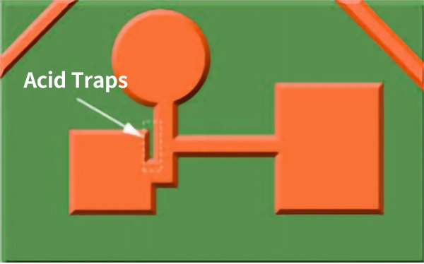
What are the characteristics of wet etching?

Pros of Wet Etching Cons of Wet Etching
1.Cheaper. 1.Pattern etching fidelity is not ideal.
2.It breeds excellent surface uniformity. 2.Isotropic etching.
3.Better adaptability. 3.PCBtank board etching patterns are difficult to control the fine lines.
4.It is impeccable in its selectivity and is therefore mainly used for etching on the inner surface for accuracy. 4. Covering Toxic chemicals.
5.Higher etching rates. 5.Risk of contaminating water.
6.Equipment for wet etching is easy to maintain.
7.Wet PCB etching can also be performed in normal atmospheric environments.

Understand the process of PCB etching solution.

When manufacturing a PCB, a layer of copper is added to the substrate. Sometimes, both sides of the substrate are covered with a copper layer. A PCB etching process is performed to remove excess copper, leaving only the required copper traces after the etching process.
Although there are these different etching methods, the most commonly used etching method is the use of hydrochloric acid or ferric chloride. Both chemicals are readily available and economical. The main purpose of the PCB copper etching process is to track the circuit design on the copper plate. To do this, you need to follow a few steps as follows:

Easy PCB Etching Step
StepsDetailed
Step 1Design the board. Note: Remember to reverse the circuit diagram you designed so that the printed circuit diagram is not reversed.
Step 2Print the design onto the transfer paper.
Step 3Polishing the copper plate to make the surface rough so that the transfer paper adheres better. Note: Remember to use surgical gloves to handle copper plates and etching solutions.
Step 4Wipe the copper plate with water and rubbing alcohol and dry it.
Step 5Put the transfer paper onto the copper plate.
Step 6Pass the copper plate through the laminator 5-7 times until the plate heats up.
Step 7After passing through the laminator, put the plate into a cold bath and stir until the paper floats.
Step 8Place the PCB into the etching solution in the PCB etch tank and stir until the unwanted copper is dissolved.
Step 9Dissolve the copper and rinse in a water bath, dry and wipe off the ink on the PCB with rubbing alcohol.
Step 10Now you have an etched PCB board, but still need to drill holes.

What are the differences between single-sided, double-sided and multilayer PCB etching?

Single-sided PCB boards are made of rigid laminates with copper varying thicknesses on one side. Double-sided PCB boards have copper on both sides of the laminate. There are copper foils on the top, bottom and inner cores of multilayer PCB. Therefore, the PCB etch solution differs in different types of PCB. We have introduced the etching way of single-sided PCB above in details. So we will brief other two etching ways.

Multi-layer PCB etch: The inner layer imaging process for a multilayer PCB consists of several stages. In the first stage, the inner layer passes through a chemically prepared line that forms a roughness on the copper surface, which is necessary for optimal adhesion of the photoresist. In the next stage, use a hot roller to pass the panel through the automatic lamination line and then apply the dried photoresist film to the panel. After cooling, the panels are collected on a shelf and transferred to the exposure process, i.e. selective photoresist exposure, which occurs on a direct laser imaging system. Leave the exposed panel for a period of 15 minutes and then transfer to the development area. The unexposed photoresist fraction dissolves in the developer solution and the exposed copper is removed. Then the final stage is the quality check, transferring the panel to the etching of the inner layer.

  • Single-sided process: blanking and grinding edge→ drilling→ outer pattern → (full plate gold plating) → etching → inspection.
  • Double-sided process: blanking and grinding edge→ drilling→ sinking copper thickening→ outer pattern → tin plating, etching and de-tin → secondary drilling → inspection.
  • Multi-layer PCB boards process: blanking edge →drilling positioning hole→ inner layer pattern→ inner layer etching → inspection→ blackening → laminated → drilling→ sinking copper thickening→ outer pattern → tin plating, etching and de-tin → secondary drilling → inspection.

How to clean the PCB after etching?

Usually the circuit is chemically etched on the assembly line and cleaned immediately, and the etching and cleaning are carried out simultaneously on the same assembly line. However, depending on the etching process, different cleaning methods will be used. Usually wet etching will be strictly controlled when chemical etching copper traces. Avoid unnecessary blemishes and etching incompleteness.
This can be perfectly guaranteed on the JHD etching line. Usually only distilled water is required for simple cleaning. Dry etching, on the other hand, does not require any chemicals to be cleaned and dried. Fully automatic plasma etching and laser etching machines can be molded in one go with precise computer control.
JHD is particularly concerned with the quality of the printed circuit board etching process. The professional skills and training of employees will be reviewed regularly. Continuously introduce high-precision automation equipment to ensure the accuracy of etching.

Hazards of PCB Acid Traps.

After etching, the PCB sometimes has an acid trap problem. This is because the solution used for etching is not completely cleaned, and the circuit is damaged to a certain extent. Acid traps can affect the performance of the resulting PCB.

  • Effects on traces:
    Copper traces will be greatly affected by acid traps. The acid seeps into the traces to form isolation zones and travel to the rest of the circuit. Gradually, the motherboard disconnected.
  • Effects on vias:
    One of the areas where acid can penetrate is through holes. If this happens to vias that do not have tents, the acid will attack them. Damage can be minimized if the designer has plugged or tented the vias. Unfortunately, if they were open, the acid could seep into the other side of the board and damage the components on that end. Damaged components are visible on both sides. Vias that are not kept a sufficient distance from each other can be particularly vulnerable to this damage. A sufficient gap from each other to reduce possibility of acid trap is a useful way. Click to view detailed PCB through hole coverage knowledge.
  • Effects on connectors:
    The connectors are soldered to pads which are basically copper sheets. Component connectors can also be affected if acid flows to the pads.
  • Effects on solder maskers:
    The solder masker will get eroded by exposure by acid traps.

How can acid traps be prevented?

An acid trap is an area of ​​a PCB that contains aggressive chemicals that should be flushed away. Acid traps can damage copper traces as well as nearby components and cause board defects. Acid traps can be especially detrimental to multilayer boards if the acid passes from the trap through open holes and other parts of the board. Additionally, leaking etch acid can damage component connectors and surface mount components. Generally, we eliminate all 90 degree angles in the wiring design and check the gaps at the connection with a minimum of 3 mils.

PCB Acid Traps

Merest space between traces, vias, and pads: The smallest clearance between the traces or vias and the edge of the board allows the corrosive solution to penetrate the traces and eventually cause breakdown. Another major problem is that copper can easily corrode when the traces are thin. For this case you can use the design tool to calculate the correct spacing value and then change it accordingly to reduce the possibility of acid traps, and you can also prevent this with tents and blockages to minimize damage.
Isolated Copper Zones: Abandoned copper areas are called Copper Islands or Dead Copper. This part is not etched and it is easy to retain the solution. Advanced design tools can help you remove these dead spots. This also needs to be taken seriously.
DRC error: Sometimes, however, in these tools, small gaps and traces of the connection angle to acute inclusion are also not found. Therefore. It is crucial to set the correct settings and carefully review the design rules.

Here are some basic preparations and maintenance to help you protect your design from acid traps and the damage they cause.  

Patient, carefulness and good techniques are requested in PCB etching, which is of much importance in manufacturing PCBs. JHDPCB already have a complete set of PCB etching method with fineness and efficiency. We strive to meet every client’s need and to produce satisfying products. If you are interested in our PCB services, please contact us.

Get a PCB Quote Now

Open high-quality PCB manufacturing services in JHDPCB

Leave a Comment