Why choose JHDPCB?
- Real PCB and PCBA manufacturers;
- Meet industry certification and production standards;
- 99% delivery on time;
- 10+ years of industry experience;
- 150+ experienced R&D team;
- 5000+ orders/day;
contact us
Provide quality service for your PCB project. Tel: +86 755 2753 9533
HDI PCBs
What is HDI PCB?
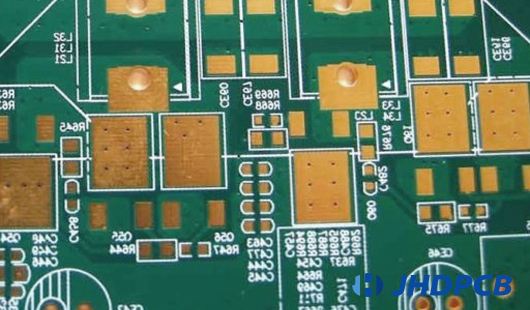
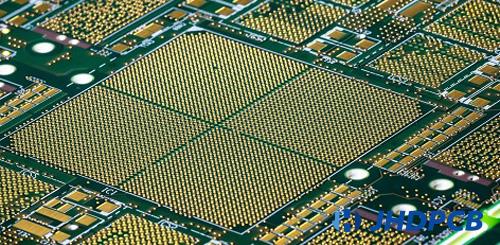
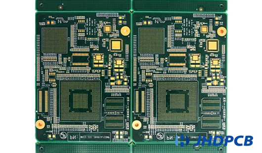
High Density Interconnect (HDI) PCB is one of the very popular technologies in PCB. Due to its higher circuit density than traditional circuit boards, HDI PCB designs can include smaller through holes and capture pads, as well as higher connection pad density. HDI boards contain blind and buried vias, and usually contain microvias with a diameter of 0.006 or smaller. This makes it possible to achieve more functions on less board area through some technologies.

Features of HDI PCB in design and manufacturing:
By using HDI technology, HDI PCB has thinner lines, smaller holes, and higher density than traditional PCBs. Designers can now place more components on both sides of the original PCB as needed. At the same time, with the development of through-hole and blind-hole technology in pads, it allows designers to combine dense component placement and finer circuits. This means that the signal transmission speed is faster, and the signal loss and cross delay are significantly reduced. HDI PCB uses laser drilling, while traditional PCB usually uses mechanical drilling. Laser drilling allows the aperture to be smaller and the size is between 3.0-6.0mil, which can save a lot of pad space and achieve more layouts per unit area.

HDI PCB often appears in high-tech products such as mobile phones, touch screen devices, notebook computers, digital cameras, 4G network communications, and of course, it is also prominent in medical equipment.
Advantages and applications of HDI PCB
· Compact design
The combination of micro vias, blind vias and buried vias greatly reduces board space. With the support of HDI technology, a standard 8-layer through-hole PCB can be simplified to a 4-layer HDI PCB with the same functions.
· Reduce interference inductance and capacitance effects, excellent signal integrity
By using small vias, all stray capacitance and inductance will be reduced. The combination of bind vias and via-in-pad technology helps to shorten the length of the signal path. These will lead to faster signal transmission and better signal quality.
· High reliability
HDI technology makes wiring and connection easier, and provides PCBs with better durability and reliability under hazardous conditions and extreme environments.
· High cost performance
If the traditional pressing process is used, when the board exceeds 8 layers, more manufacturing costs are required. But HDI technology can reduce costs and maintain functional purpose.

The birth of HDI PCB has brought more diversity to portable electronic devices, and it has also brought more challenges to PCB manufacturers. In order to adapt to the trend of miniaturization and multi-functionalization of electronic products, JHDPCB has done a lot of work for the professionalism of employees while improving the level of equipment. You can rest assured to provide us with HDI design, we will provide you with satisfactory services and HDI products.


