DIP Package

directory

What is a DIP package?

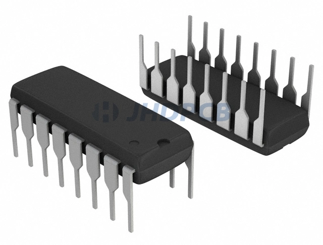
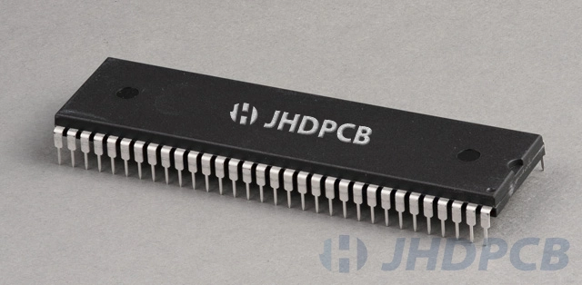
Dual in-line package (DIP) is the most common through-hole IC package in the PCB electronic component packaging process, abbreviated as DIP or DIL. DIP packages are typically melt-molded from an opaque epoxy resin with a lead frame supporting the device chip. And provide connecting pins extending vertically out of the rectangular plastic housing. Silver, gold or tin plating is optional around the parallel metal pins (pin headers) on both sides of the IC.

DIP packages can be mounted on a circuit board or inserted into a socket using through holes. DIPs are often referred to as DIPn, where n is the total number of pins. For example, a through-hole IC package with two rows of eight pins would be a DIP16. Common packages range from 3 to 64 or even 100. DIP derives a higher density package form – SDIP (Shrink DIP), which has six times the pin density of standard DIP.
The number of pins determines the overall size of the DIP package. The most common stitch counts are four, six, eight, ten, twelve, fourteen, sixteen, eighteen, twenty, twenty-eight, and forty, among others. The pins on the DIP IC have different pitches such as 0.5mm, 0.65mm, 1.27mm, and 2.54mm. Regular Standard Pitch – Ideal for loading into breadboards, veroboards and other prototype boards. Of course, there are also some special pitches in some special DIP package series.

Dual in-line package (DIP)

History development:

Dual-in-line assembly was invented in 1964 by Bryant Buck Rogers, Rex Rice, and Don Forbes of Express Semiconductor. At that time, the small number of pins of electronic components on the circuit limited the use of integrated circuits. A more complex circuit requires more power leads and more signals. The shape of the early components was circular, and it was gradually optimized to a rectangle to increase the density of PCB components. DIP components are also well suited for automated assembly equipment. All components are soldered by wave soldering equipment and then inspected with automatic testing equipment. Only a small number of manual operations are required to save labor costs.

Due to the relatively large size of DIP package components. In the 1990s, DIP packages were commonly seen in more than 20-pin assembly processes. But by the end of the twentieth century, with the popularization of ISP technology. DIP packaging is gradually replaced by the small size and weight advantages of SMT packaging. The surface mount process avoids the cost of extensive drilling and improves the high-density interconnection of circuit boards.
However, the DIP package is still popular with hobbyists due to its low cost and simple operability. At the same time, in some special applications, DIP package components will still be used. For example, it is inconvenient to use surface mount technology components when making PCB prototypes. We use DIP components with adapters, and the resulting prototype boards are reworkable and ready to plug and unplug components.
DIP packages were very popular in the early days when electronic components were plugged directly into the motherboard.

What are the different types of DIP packages?

There are many different IC types in DIP packages, mainly divided into the following categories:

  • PDIP: Traditional Plastic Dual In-Line Package;
  • SDIP: Skinny Dual In-Line Package;
  • SPDIP: Shrink Plastic Dual-In-Line Package;
  • Cer DIP (Ceramic): Glass Ceramic Sealed type;
  • SC DIP (Ceramic): Single-layer Ceramic Dual-in-line DIP;
  • MC DIP (Ceramic): Multilayer Ceramic Dual In-Line DIP;
  • CerDIP Side Brazed: Side Brazed Ceramic Dual In-Line Package;
  • Metal or Hybrid DIP: Mixed metal dual in-line DIP, sealed and unsealed;

Plastic Dual In-Line Package (PDIP) is the most common type of DIP package. Its rectangular housing is made of plastic. It is formed by fusing and gluing the plastic around the leads. But due to the porous nature of plastic, it is not hermetic. Most DIP packaged chips use thermosetting resin plastics. Its ultra-short curing cycle can produce hundreds of chips in a short time.
Plastics or ceramics are generally used in the dual in-line packaging process of high-reliability equipment. The ceramic package has good air tightness.

How to install DIP package?

Before the DIP package, it is necessary to drill holes in the reserved positions, and the number of through holes corresponds to the number of pins. Components can have pins inserted into the holes and fixed to the board by soldering. Its operation is very simple, of course, care needs to be taken in the process of removing and inserting chips to prevent damage to the pins.

In addition to the normal hole-punch mounting, mounting via DIP sockets is also possible. The DIP IC can be easily removed or installed from the circuit board using the socket. Especially the PCB prototyping process is used frequently. At the same time, problems such as solder bridges caused by overheating of components during the soldering process can be avoided. DIP packaged components can be used in conjunction with breadboards.

Features of DIP package.

The dual in-line package is characterized by easy perforation soldering of printed circuit boards and good compatibility with circuit boards. However, due to the gradual high-density interconnection of electronic devices, the limited number of pins in the DIP package cannot achieve small-scale high-density integration. Now, DIP has slowly faded out of people’s field of vision.

Spacing:
The internationally accepted DIP package JEDEC standard has a pitch of 2.54 mm between two pins. The DIP package used in some Eastern European countries is slightly different from the JEDEC standard, and its pitch is metric 2.5mm. The distance between the two rows of pins depends on the number of pins. Other less common distances are: 1.78 mm, 7.62 mm, 15.24 mm, 10.16 mm or 22.86 mm.

Number of needles:
The number of pins in a DIP package is always an even number. Common DIP pin counts are 8, 14, 16, 18, 20, 24, 28, 32 or 40, 48. Of course, there are also 52- or 64-pin packages, which are the maximum pin counts commonly used in DIP packages today.

Orientation and Pin Numbers:
When the identification notch of the DIP component is facing up, the first pin on the upper left is pin 1, and the other pins in the same row are sorted in anti-clockwise order. Jumping to the opposite row of pins after going to the bottom is to sort from bottom to top.
Take the DIP18 integrated circuit as an example: when the identification notch is facing up, the pins on the left are 1-9 pins from top to bottom, and the pins on the right are 10-18 pins from bottom to top.

Plastic Dual In-Line Package

Dual in-line package data parameters.

DIP Package data parameter table
DIP package seriesCDIPCDIP BBCDIP SBPDIPSDIP
Number of pins8~4014/188~648~648
Spacing (mm)1.78/2.542.541.78/2.542.540
Height (mm)4.0~9.754.07/3.752.35~7.433.302~7.754.445
Length (mm)9.6~52.0720.07/25.210.29~82.579.53~66.558.255
Width (mm)6.67~28.9612.457.37~22.746.35~21.598.255

Fields of application of DIP packages.

In the past, DIP packages were often used in many digital ICs. DIPs are often seen on older VGA/SVGA graphics cards or BIOS chips. DIP packages are also frequently used in modern assembly of electronic components such as transistors, switches, light-emitting diodes, and resistors. Other common DIP package parts include:

  • DIP switch;
  • LED;
  • Bar display;
  • Seven segment display;
  • Relay;
  • Computer.

What is SOP (SOIC)?

SOIC stands for Small Outline Integrated Circuit, which belongs to one of the series of SMT packaging technology. Small Outline Package has two abbreviations: the American JEDEC standard is called SOIC. The JEITA standard in Japan is called SOP. American SOIC is wider than Japanese SOP.

SOIC package: All pins are bent out and reduced in size. Each pin is typically about 1.27mm apart from the next.
SOP package: SOP is basically similar to SOIC and is a smaller SOIC package version. It has a smaller form factor with a pin pitch of less than 1.27mm.

Small outline IC package type.

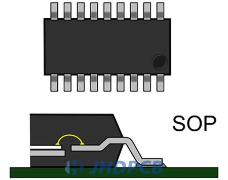
SOP generally refers to a series of packages, including SSOP, TSOP, TSSOP, MSOP, QSOP, etc.

  • The lead spacing on both sides of the SSOP (Shrink Small Outline Package) package is less than 1.0mm.
  • The width of the TSOP (Thin Small Outline Package) package is greater than 300mils, and the total height is less than 1.2mm.
  • The TSSOP (Thin-Shrink Small Outline Package) package has a package width of less than 300 mils and an overall height of less than 1.2 mm.

SOIC package

Common Prefixes for SOP Package Series
AbbreviationWord meaning
Cceramic
Pplastic
Sshrink
Ppower
Tthin
HHeat sink
QQuarter size
HHermetic sealed
Vvery
Nnarrow
Wwidth
M,U,μmircro
EPExposed pad

DIP package VS SOP package.

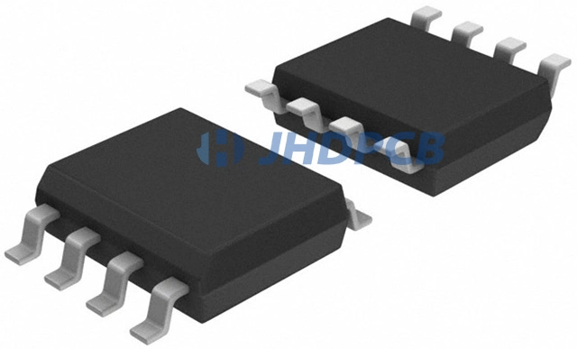
Both DIP and SOP belong to package types with two terminal directions. The package methods of Small Outline Package and Small Outline J-leaded series are basically similar to DIP. Unlike DIP package in-line terminals, SOP’s terminals are L-shaped. It is just that the terminal shape of the DIP in-line linear takes up a large space. Compared to the DIP package with the same number of pins, the SOP package is smaller in size. SOP reduces the thickness by more than 60% and saves 30%~45% of the space. Therefore, SOP can be regarded as a scaled down version of DIP package. It is a common surface mount technology commonly used in consumer electronics and PCs. View more PCB package types.

SOP package

Application areas of SOP package.

Some products in Small Outline Integrated Circuits (SOICs) require less power than DIPs of the same efficiency. Therefore, it is often used in some application scenarios with special requirements for low power:

  • Consumer Electronics;
  • RAM;
  • Mobile phone;
  • PC equipment;
  • Car;
  • Photoelectric components;
  • Controller;

Advantages of SOP packaging process.

The biggest advantage of the small outline integrated circuit is its small size, so it can be assembled on a smaller size PCB circuit board. At the same time, less material is used in the encapsulation process. To a certain extent can also the manufacturing cost of IC.

  • 100% Sn;
  • Green materials are standard – lead free and RoHS compliant;
  • Standard package form factor;
  • Multi-chip production capacity;
  • Turnkey testing services;

To learn more about the type of PCB package, you can learn about it through the blog of the JHD package series. If you are not sure which assembly method should be used for your newly designed PCB product to ensure its stable operation, you can consult our professional customer service team.