Mixed assembly
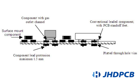
Although surface mount technology SMT has become the dominant placement method in PCB manufacturing, there are still some components that are not suitable for SMT assembly. At this time, it is necessary to apply SMT assembly, THT assembly and BGA package on the same board. This combination of assembly techniques is called hybrid assembly, and no solder paste is used in the manufacturing process.
Most components are soldered on the board in a surface mount configuration, but for some components that cannot be used in SMT processes, hybrid PCB assembly is required.
What is a mixed assembly?
Mixed technology PCB assembly utilizes surface mount technology (SMT), through-hole technology, and ball grid packaging (BGA). In other words, it is a combination of Surface Mount Devices (SMD), through-hole components and ball grid packages. It combines the best of three mounting technologies and is often used in applications of mixed requiring a combination of these three types of components. The biggest advantage of this kind of PCB assembly is that there is no need to use any solder paste, which can effectively solve any problems in soldering.
What are the advantages of hybrid assembly?
A relatively new approach in the PCB manufacturing industry is hybrid assembly printed circuit board, which offers the following advantages:
- It can mount through-hole, SMT and BGA components on PCB.
- Single or Double Sided Hybrid Technology or SMT (Surface Mount) Single or Double Sided BGA and Micro BGA for PCB assembly
- 100% X-ray inspection for ease of installation and rework
- PCB board components: including various BGA, QFN, CSP, 0201, 01005, POP, small batch Pressfit Components
- Polarized capacitors: SMT polarized capacitors, through-hole polarized capacitors
- Rework Capabilities: Removal and Replacement of BGAs and MBGAs, Experienced in Ceramic and Plastic BGAs, Rebalino BGAs and MBGAs
- They provide the ability to combine RF and digital electronic designs on a single PCB.
- They help miniaturize and reduce overall electronic package size and reduce or eliminate cables and wire harnesses.
- Known for improving reliability.
- Known for its high cost performance.
- Light weight and high precision
- increase stress resistance
Which packaging processes are commonly used in hybrid assembly technology?
THA
In traditional Through-Hole Assembly, a through-hole or wired component is put in a hole drilled and then secured to the contact pads using soldering techniques. These components differ from surface mount components in that they are connected by running the leads “through” the holes in the board from the other side of the board.By the late eighties, the technology still dominated the industry. THT has some sway in today’s electronics manufacturing market, although SMT assembly methods have replaced a large portion of the more expensive, labor-intensive traditional assembly processes. There are still many types and situations in which THT is used, including large components (e.g. inductors, capacitors), components with high mechanical stress (switches, connectors) and high performance electronics (e.g. relays or high voltage resistors). It offers specific advantages that keep it relevant. The bonds formed between THT components and circuit boards are much stronger than SMT bonds, making THT ideal for components subject to mechanical and environmental stress or high temperatures. Through-Hole Assembly are also easy to change in case of prototyping, making them ideal for testing and amateur users.
BGA
An advanced packaging technology in SMT assembly is called BGA. BGA is a product of the development of electronic technology and marks a major advancement in packaging technology. The surface of the tube has many spherical bumps, which can realize high-density packaging. The BGA package can simultaneously make the single-chip module more powerful and also reduce the package size. The greatest advantage of BGA assembly lies in high-density PCB products. First, BGA assembly allows ICs with hundreds of pins to be packaged in small packages, allowing more functionality to be integrated while utilizing less space. Second, BGA packages have excellent electrical properties and thermal conductivity. Third, its better solderability leads to good manufacturing yields. Owing to these benefits, BGA components have been widely used in wireless, medical industry, LED industry and satellite, aerospace, telecommunications and military and other fields.
SMT
SMT assembly is the process of installing electronic components on a PCB by soldering. The process simply involves soldering the leads of the part to the pads on the PCB with a small amount of melted solder paste. It usually involves positioning and mounting components onto a PCB using automated equipment. MT brings many benefits to PCB assembly. Automated equipment not only can quickly install parts, but also can increase production and reduce manufacturing costs. It has the ability to use smaller components that are more compact and lighter than through-hole components. This enables engineers to maximize space on the PCB and reduce product size without compromising functionality or performance. Besides, producer can make it easier to carry through reducing the weight of the product. The ability to use higher power components, high component density, smaller footprint and lower weight. At the same time, it also makes the PCB assembly process simple and reliable.
Design rules for component placement in mixed assembly.
PCB design rules for component placement in mixed assemblies, pay attention to the following points:
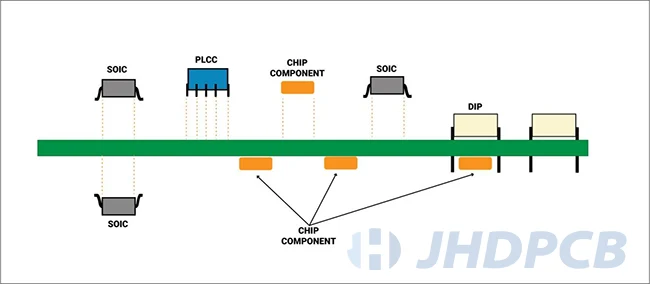
- Try to put all the components on the same side as much as possible, which can also make it look less confusing and save space.
- If there is no way to satisfy all the components on the same side, then it is best to mount the surface mount SMT components on the underside of the board as much as possible.
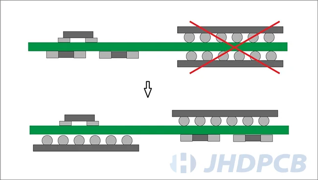
- Never allow two BGA components to face each other.
- To help with future needs and to avoid re-soldering the BGA, take care to allow a 5 mm clearance between the BGA assembly and any passive components on the board.
- Try not to place the BGA device and the THT component too close together.
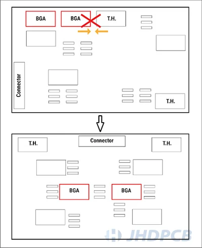
- Because large and heavy components placed on the edge of the board can cause the board to bend, pay attention to the weight distribution of the entire board.
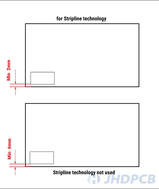
- Pay attention to the gap between the edge of the board and the components. If stripline technology is used, the gap is 2 mm; if stripline technology is not used, the gap is 4 mm.
- Use the same package size as much as possible. This may not be useful every time, but it helps to optimize the installation process.
Taking these factors into consideration, PCB hybrid assembly can be efficiently performed. Facts have proved that choosing a hybrid assembly has advantages over choosing a specific installation technique.
Application of Hybrid Assembly Technology.
Our JHDPCB uses a variety of first-class equipment. This helps us to provide high-quality PCBs that are performance oriented. We regularly meet assembly requirements for complex hybrid models for customers in the defense, aerospace, petroleum, medical and computer, gas, power production, telecommunications and transportation industries. The following are some of the main and most common applications of our hybrid model PCB components:
- LED lighting products
- Server motherboard
- video processing
- Communication hardware
- Sensor board
- Industrial controller assembly
- Smartphone accessories
- processor
- Automatic temperature control system
- Timer based sprinklers
- Acoustic scanning microscope
- Automatic dispensing machine
- Template printing machine
What are the precautions for mixed assembly?
Design for assembly(DFA) provides a foresight pointing out the complexities that may arise before the actual assembly process takes place. Without proper planning,the assembly might not match the actual design requirements. Unlike DFA,design for manufacturing(DFM) does not consider the possible difficulties that may arise during the placement of components. Once DFM is completed,we are just left with a bare board on which the components are to be assembled. Before assembling them, we must decide on the following aspects:
1. Types of components used-
Even though SMDs are used in abundance in PCBs today, there are components that are not suitable for SMT mounting. That is why it is best to apply both technologies on the same circuit board. This ensures all the benefits of SMT like high precision, lightweight, and easier automated mounting along with the THT advantages like robust connections and high stress tolerance.
SMT and THT require different soldering methods. Surface-mount components undergo reflow soldering and through-hole components are subjected to wave soldering /manual soldering.
2. Automated/manual placement-
You need to choose the appropriate component placement type based on the actual situation. The following are the advantages and disadvantages of automatic placement:
Advantages of automated placement:
- Fast
- Consistent and accurate
- Reliable and offers high quality
- Low cost for big volumes of the product
Disadvantages of automated placement:
- Lack of precise control while placement
- Not suitable when dealing with low volumes
- Complications may arise with component leads
The above disadvantages should be fully considered when choosing a placement method. In the case of small assembly batches, the cost required to set up automated placement can be high. In such cases, always opt for manual placement.
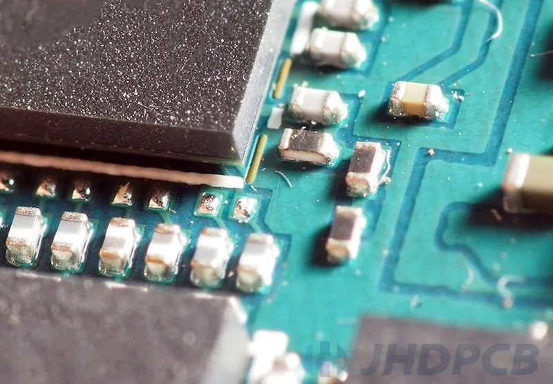
Mixed assembly technology capabilities of JHDPCB.
Hybrid assembly is a combination of automated and manual assembly processes. During PCB mixed assembly, some components need to be inserted manually, while the rest are inserted using pick and place machines. This process can be finished in double-sided or single-sided PCBs with multi-layer components. In JHDPCB, we have many years of experience in manufacturing and assembling various PCBs. Our capabilities in hybrid model assembly services mainly include four aspects:
Complete traceability: We ensure to provide you with complete PCB traceability, from the ordering process to the final product delivery to you.
Rapid prototyping: Rapid prototyping is one of our core competitiveness. We provide facilities equipped with NPI and prototype production lines and the ability to ask for your services at any time.
Cutting edge equipment: We have professional equipment in the market, which can provide you with rapid production build and prototype. We have the most advanced automatic assembly equipment, automatic laser aiming and flux dispensing, fast mounting machine for ultra small and ultra-thin chip components, wave soldering machine, etc.
Inspection: We have our own internal inspection laboratory, equipped with advanced tools and equipment. We have a team of qualified and experienced people who can check your PCBs to see if they meet your specifications and the industry standards needed to adopt these technologies.
It includes: pre flow inspection, solder paste inspection, X-ray inspection, function test, AQL inspection for final assembly, etc.
We understand the importance of fulfilling orders on time. As a result, we can offer you a fast turnaround time, reducing time to market and giving you a competitive advantage. As a mixed assembly manufacturer, we are able to provide mixed technology PCB assembly services, including double sided mixed PCB assembly services, and we can easily handle high-mix complex pcb assemblies. In addition, we are also fully capable of providing prototype quantities and volume production to meet all your volume requirements. Our experienced team will share a custom quote and ensure PCB fabrication meets your exact needs.
We believe that when you partner with us, you gain access to a wealth of industry best practices and advantages. Among many mixed assembly manufacturers, choosing JHDPCB must be the most correct decision for you.


